How Does the RO3035 Laminate's Thermal Stability Enhance PCB Reliability?
How Does the RO3035 Laminate's Thermal Stability Enhance PCB Reliability?
In high-frequency electronics, heat is an inevitable byproduct of operation. Components like power amplifiers (PAs) in cellular base stations or automotive radar modules generate significant heat. If the PCB substrate is not stable, this heat can cause catastrophic failures. The RO3035 laminate is engineered to prevent these failures through several key mechanisms:
1. Matched Coefficient of Thermal Expansion (CTE) Prevents Mechanical Failure
One of the most critical aspects of thermal stability is how much a material expands and contracts when heated or cooled.
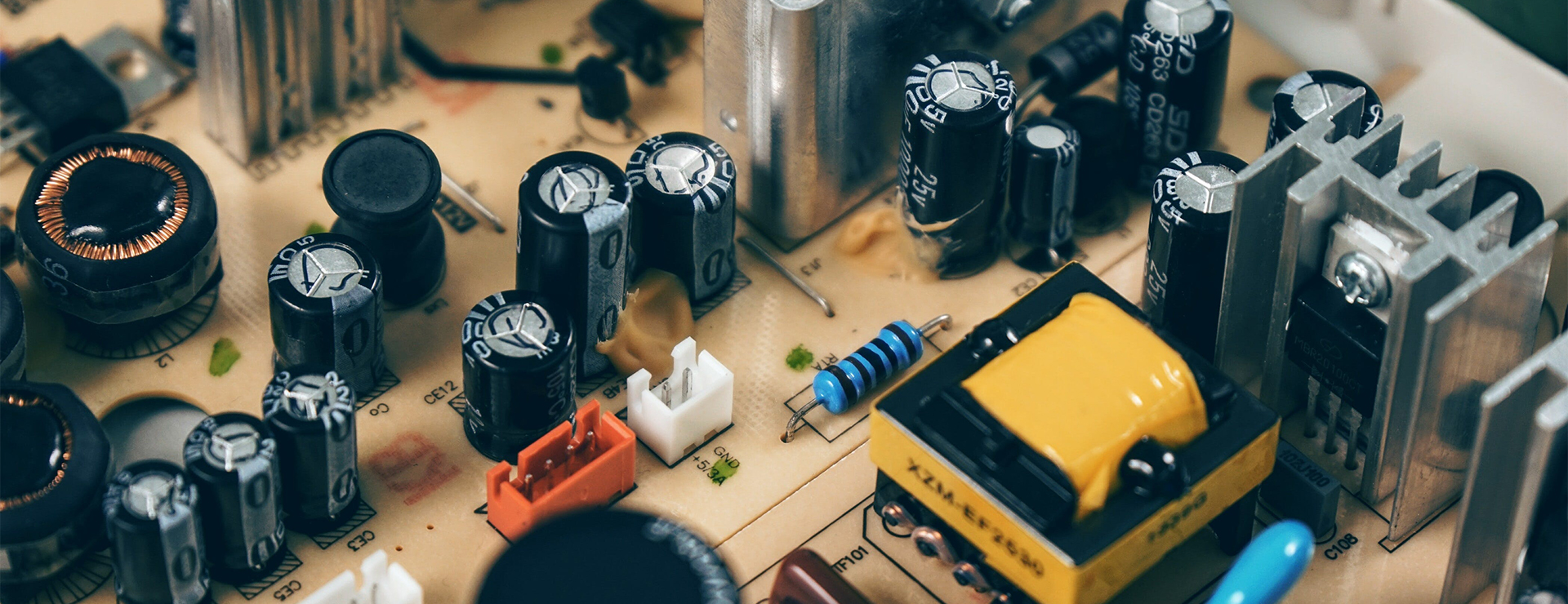
The Problem: If the PCB laminate expands at a significantly different rate than the copper traces and plated through-holes, it creates immense stress. This can lead to cracked vias, broken circuit traces, and delamination (separation of the copper from the substrate). For a board with 21 vias and 63 pads, as in our standard offering, via integrity is paramount.
The RO3035 Solution: RO3035 has a low and well-controlled in-plane CTE:
- X & Y Axis: 17 ppm/°C
- Z Axis: 24 ppm/°C
Crucially, the in-plane CTE (17 ppm/°C) is very close to that of copper (≈17 ppm/°C). This "CTE match" means the substrate and the copper circuits expand and contract in harmony during thermal cycles.
Reliability Enhancement: This drastically reduces mechanical stress on the plated through-holes and the copper-to-laminate bond. It prevents via barrel cracking and pad lifting, which are common failure points in less stable materials, ensuring the electrical connections remain intact over thousands of thermal cycles.

2. High Decomposition Temperature (Td > 500°C) Ensures Material Integrity
During assembly and operation, theRogersRO3035 PCB is subjected to high temperatures.
- The Problem: Standard FR-4 materials have a lower glass transition temperature (Tg) and can begin to decompose at soldering temperatures, leading to blistering, delamination, and a loss of mechanical strength.
- The RO3035 Solution: RO3035 is a ceramic-filled PTFE composite with an exceptionally high Decomposition Temperature (Td) exceeding 500°C. This is far beyond the peak temperatures encountered in typical lead-free soldering processes (which are around 240-260°C).
- Reliability Enhancement: The board remains mechanically and chemically stable during all assembly stages and throughout its operational life. This guarantees that the 0.37mm thin board will not warp, blister, or degrade when subjected to the heat of soldering components or from internal power dissipation, ensuring the physical integrity of the assembly.
3. Stable Dielectric Constant (Dk) Over Temperature Maintains Electrical Performance
For high-frequency circuits, electrical stability is just as important as mechanical stability.
- The Problem: In many materials, the Dielectric Constant (Dk) can shift significantly with temperature changes. For a circuit designed to operate at a specific frequency (e.g., 24 GHz for automotive radar or 28 GHz for 5G), a drifting Dk causes a shift in the impedance and the resonant frequency. This leads to signal distortion, loss of gain, and overall system performance degradation.
- The RO3035 Solution: Rogers 3035 offers a remarkably stable Dk of 3.50±0.05 across a wide temperature range. This is a core feature of its "thermal stability."
- Reliability Enhancement: Your circuit's performance remains predictable and consistent whether it's a cold start in winter or operating at peak load on a hot summer day. This is non-negotiable for applications like global positioning satellite antennas and cellular power amplifiers, where signal integrity is critical.
4. Low Dissipation Factor (Df) Minimizes Signal Loss and Heat Generation
The electrical properties of the laminate also contribute to thermal management.
- The Problem: At high frequencies, materials with a high loss tangent (Df) convert significant signal energy into heat. This self-heating effect can raise the board's local temperature, creating a feedback loop that further degrades performance and stresses components.
- The RO3035 Solution: With an ultra-low Dissipation Factor of 0.0015 at 10 GHz, RO3035 minimizes dielectric losses.
- Reliability Enhancement: Less signal energy is lost as heat. This results in a lower operating temperature for the PCB itself, which directly increases the mean time between failures (MTBF) for both the board and the surface-mounted components. This is a key benefit for power amplifiers, where efficiency and heat management are major design challenges.
Conclusion: A Synergistic Effect for Ultimate Reliability
The thermal stability of the RO3035 high frequency laminate is not a single property but a synergistic combination of its matched CTE, high Td, stable Dk, and low Df. For our RO3035 2-layer 10mil Immersion Gold PCB, this means:
- Mechanically Robust: It can withstand the rigors of assembly and harsh operating environments without suffering from cracked vias or delamination.
- Electrically Predictable: Its performance remains locked in, ensuring that your high-frequency design works as intended throughout its lifespan.
- Thermally Efficient: It runs cooler and manages heat more effectively, leading to a more reliable end-product.
This holistic thermal stability is precisely why this RO3035 10mil PCB is specified for the most demanding applications in the automotive, aerospace, and telecommunications industries, where failure is not an option. By choosing a PCB built onRO3035 substrate, you are not just buying a board; you are investing in long-term, predictable performance.