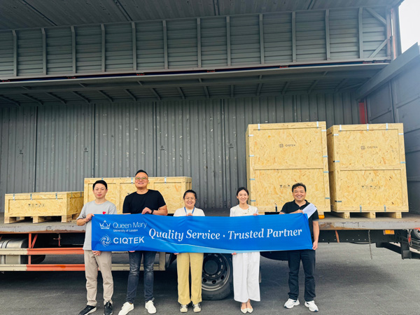
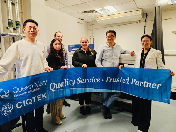
CIQTEK is excited to announce our participation in ARABLAB 2025, one of the leading international trade shows for laboratory technology, scientific instruments, and petroleum exploration equipment. The event will take place from 23 to 25 September 2025 at the Dubai World Trade Center, UAE, and visitors can find us at Booth H1-C24, Sheikh Saeed Hall 1.


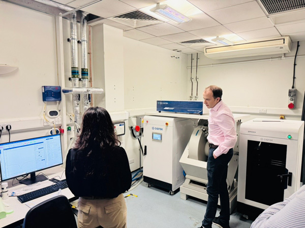
At the exhibition, CIQTEK will present our latest innovations in electron microscopy (FIB/SEM, TEM), electron paramagnetic resonance (EPR) spectrometers, BET Surface Area &Porosimetry Analyzers, and other advanced analytical instruments. The team will demonstrate product capabilities, share real-world application success stories, and discuss solutions for researchers and industrial professionals across multiple sectors.


In addition, CIQTEK will introduce QOILTECH, our specialized brand for innovating petroleum exploration and oilfield services. QOILTECH focuses on the R&D, manufacturing, and sales of petroleum exploration equipment, including RSS, MWD/LWD, resistivity, and near-bit azimuth gamma tools, designed for extreme environments. With proven expertise in tool design and application, QOILTECH delivers equipment capable of operating at depths of up to 100,000 meters annually, supporting efficient and reliable petroleum logging while drilling operations.


QOILTECH oilfield services


ARABLAB provides a key platform to connect with industry experts, researchers, and distributors from around the world. CIQTEK looks forward to engaging with attendees, showcasing how our advanced scientific instruments and petroleum exploration tools can drive breakthroughs in research, industrial applications, and oilfield operations.

We warmly invite you to visit our booth at H1-C24 to experience our instruments in action and speak directly with our product specialists.

Event Details:


  • Date: 23–25 September 2025

  • Venue: Dubai World Trade Center, UAE

  • Booth: H1-C24, Sheikh Saeed Hall 1

In industrial automation, robotics, and precision instruments, connector performance is often the “invisible bottleneck” that limits system reliability. Traditional connectors can be hard to route in tight spaces, difficult to service, and prone to interference. WAIN’s MI Series miniature high‑density connectors give engineers a space‑saving, easily maintained, high‑reliability alternative.

MI Series Miniature High‑Density Connectors


Break the Space Barrier 


· MI connectors feature a compact form factor that is smaller than conventional products while integrating three functional modules—signal, power, and brake—into a single unit. This eliminates cable clutter and frees up valuable enclosure space, making the connectors easy to embed in robot joints, AGV control bays, or precision-instrument compartments.

· A partitioned, removable-module design allows users to detach either the signal or power section independently. If one module fails, the entire connector does not need to be replaced, dramatically reducing maintenance time and cost. Compared with traditional one-piece connectors, service efficiency is significantly improved.


Five Core Technology Innovations


1、One-Second Quick-Release — Latch Mechanism
MI connectors use an elastic latch-lock design that mates or unmated with a single press, cutting installation time. Anti-mis-mate coding ensures precise, reliable connections.

2、Vibration-Resistant Cold-Crimp Contacts
Contacts are cold-crimped—no soldering—delivering high-strength conductivity. Tested to withstand 500+ mating cycles, ideal for high-vibration environments such as industrial robots and rail systems.

3、360° Electromagnetic Shielding + Partitioned Isolation
Dual-layer protection:
• Outer full-metal shell blocks external EMI.
• Inner isolation chambers physically separate power and signal sections, eliminating crosstalk and guaranteeing zero-packet-loss data transmission.

4、Dual-Cable Exits for Flexible Routing
Independent power and signal channels exit through Ø 7.5 mm ports, accommodating large-gauge power and fine-gauge signal wires. The plug supports 180° dual-direction swivel, adapting to varied equipment layouts.

5、Visual Assembly — Top + Side Inspection Windows
Technicians can verify pin alignment in real time, preventing bent pins from blind mating. During service, windows enable rapid fault location, lowering technical complexity and downtime.


Proven in Harsh Environments


·Operating temperature: –40 °C … +130 °C

·Ingress protection: IP67 (mated, EN 60529) – suitable for aerospace and outdoor equipment

The open-source RISC-V instruction set architecture has rapidly evolved from a niche academic project into a global force reshaping the processor market. Over the past few years, semiconductor companies, research institutions, and startups alike have embraced RISC-V for its flexibility, reduced licensing costs, and potential for highly customized chip designs. Its adoption is accelerating in sectors ranging from data centers to low-power embedded systems, driven by the need for scalable performance and open innovation.

RISC-V processor architecture 

One of the fastest-growing areas for RISC-V implementation is AIoT (Artificial Intelligence of Things). As smart devices integrate AI capabilities at the edge, processors must handle both machine learning inference and complex sensor data processing locally. This trend is mirrored in embedded control systems, industrial automation, and edge computing platforms—where low-latency decision-making is essential. The modular nature of RISC-V allows chip designers to fine-tune cores for specific workloads, from high-performance neural processing to ultra-low-power microcontrollers.


Yet, no matter how sophisticated the processor architecture becomes, its performance is inherently tied to the accuracy and stability of its clock source. This is where crystal oscillators play an irreplaceable role. A crystal oscillator generates a precise and stable frequency signal, ensuring that instruction execution, peripheral communication, and data synchronization occur with consistent timing. Without such stability, high-speed data buses, wireless communication modules, and real-time control loops would be prone to errors and latency spikes.


In AIoT devices, for example, a small deviation in the processor clock can lead to cumulative timing mismatches between sensor inputs and AI algorithms, affecting recognition accuracy. In embedded systems such as automotive controllers or medical devices, clock instability could disrupt safety-critical operations. Even in edge computing nodes handling distributed workloads, accurate timing signals are crucial for coordinating processes across multiple devices in a network.


RISC-V processors, particularly those targeting wireless connectivity standards like Wi-Fi, Bluetooth, and 5G, rely heavily on low-jitter crystal oscillators to meet stringent communication protocol requirements. The frequency precision determines not only the processor’s internal timing but also the synchronization of RF transceivers, ADC/DAC converters, and external memory interfaces. For industrial and defense-grade applications, temperature-compensated crystal oscillators (TCXO) or oven-controlled crystal oscillators (OCXO) are often paired with RISC-V chips to maintain stability in extreme environments.


The future of RISC-V will likely see even more integration with diverse hardware ecosystems—heterogeneous computing modules, AI accelerators, and advanced security enclaves. Regardless of these innovations, every design still begins with the same foundational requirement: a reliable, accurate, and stable clock source. The crystal oscillator remains the silent but indispensable enabler, ensuring that RISC-V’s open-source vision is matched by uncompromising operational precision.


In essence, the global rise of RISC-V is not just a story of architectural freedom and innovation; it is also a reminder that at the heart of every advanced processor lies a humble yet essential timing device—without which the promise of the architecture could not be fully realized.


CIQTEK is pleased to announce its participation in the Microscopy Conference 2025 (MC2025), taking place August 31 – September 4 in Karlsruhe, Germany.

You can find us at Booth #28 in the exhibition area of Messe Karlsruhe.


MC2025 is one of the most important events in the international microscopy community, jointly organized by the German Society for Electron Microscopy (DGE), the Austrian Society for Electron Microscopy (ASEM), and the Swiss Society for Optics and Microscopy (SSOM), under the patronage of the European Microscopy Society (EMS). The conference brings together scientists, engineers, and industry leaders to share the latest advances in imaging technologies, applications, and techniques.


Exhibitor Presentation

Date & Time: Monday, September 1st, 17:10 – 17:20 pm
Location: Conference Hall, Messe Karlsruhe
Topic: Unlocking the Power of High-Speed Scanning Electron Microscopy Without Compromising Superb Imaging Resolution at Low kV

During this session, our Senior Electron Microscopy Engineer will share insights into how CIQTEK’s latest high-speed SEM technology achieves exceptional imaging resolution at low accelerating voltages, enabling breakthroughs in materials science, life sciences, and nanotechnology research.


We look forward to connecting with researchers, partners, and industry peers at MC2025. Visit Booth #28 to explore our advanced electron microscopy solutions and discuss how CIQTEK can support your work.


See you in Karlsruhe!

CIQTEK to Exhibit at MC2025 Microscopy Conference in Karlsruhe, Germany

For researchers and engineers, understanding the core specifications of a Scanning Electron Microscope (SEM) is essential for obtaining accurate results. Among the most important parameters are SEM resolution, SEM magnification, and SEM imaging modes. These three factors define the level of detail, scale, and type of information that can be captured from a specimen. Knowing how they work and how they interact helps you select the right SEM for your application.


What is SEM Resolution and Why It Matters

SEM resolution describes the smallest distance between two points that can still be distinguished as separate. It is typically measured in nanometers. Higher SEM resolution means you can capture finer details, which is critical in nanotechnology research, semiconductor inspection, and advanced materials analysis.

The main factors affecting SEM resolution include electron beam spot size, accelerating voltage, electron source type, and vacuum conditions. For example, a field emission SEM generally achieves higher resolution than a thermionic SEM. Low accelerating voltage improves surface detail for delicate samples, while low vacuum operation enables better imaging of non-conductive materials.

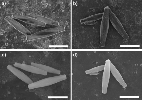
CIQTEK SEM Images


Understanding SEM Magnification

SEM magnification is the ratio between the displayed image size and the actual area scanned on the sample. Unlike optical magnification, SEM magnification is controlled electronically by adjusting the scan area. Most modern SEMs offer magnification from about 10x to several hundred thousand times, making it possible to study both large structures and nanoscale features in the same instrument.


The Link Between SEM Resolution and SEM Magnification

While increasing SEM magnification enlarges an image, the level of meaningful detail still depends on the SEM resolution. If the resolution limit is reached, higher magnification will not reveal additional structural details. For example, a system with 1 nm resolution provides much clearer images at high magnification than one limited to 5 nm.


Common SEM Imaging Modes and Their Uses

Modern SEMs feature multiple imaging modes, each designed to provide specific information:

  • Secondary Electron Imaging (SEI) – Delivers high-resolution surface topography, ideal for morphology studies.

  • Backscattered Electron Imaging (BSE) – Reveals compositional contrast based on atomic number differences.

  • Energy Dispersive X-ray Spectroscopy (EDS) – Identifies and quantifies elemental composition.

  • Low Vacuum or Variable Pressure Mode – Allows imaging of non-conductive or hydrated specimens without metal coating.

Switching between different imaging modes enables comprehensive analysis of a single sample.


Choosing an SEM Based on Resolution, Magnification, and Imaging Modes

When selecting an SEM, consider the balance between SEM resolution, SEM magnification range, and available imaging modes. High-resolution capability is essential for nanometer-scale research. A wide magnification range ensures flexibility for different sample sizes, and multiple imaging modes increase versatility for both research and industrial applications.

CIQTEK SEM


How CIQTEK SEMs Excel in Resolution, Magnification, and Imaging Modes

CIQTEK SEMs achieve nanometer-scale resolution, allowing users to observe ultra-fine surface features with exceptional clarity. This level of detail is crucial for fields such as semiconductor inspection, nanomaterials research, and precision manufacturing, where accuracy at the smallest scale determines the quality of results.


Flexible Magnification Range

CIQTEK SEMs offer a broad magnification range, enabling smooth transitions from low-magnification overviews to ultra-high-magnification nanoscale imaging. This flexibility allows researchers to locate areas of interest quickly and then zoom in for detailed examination, all without loss of image quality.


Multiple Imaging Modes in One System

CIQTEK SEM systems integrate multiple imaging modes, including secondary electron imaging for surface morphology, backscattered electron imaging for compositional contrast, and low vacuum operation for non-conductive or moisture-sensitive samples. Optional analytical tools, such as EDS, provide elemental composition data. This multi-mode capability means users can conduct comprehensive analyses without switching instruments.


High Value and Cost Efficiency

In addition to technical excellence, CIQTEK SEMs deliver outstanding value. By combining advanced electron optics, reliable hardware, and intuitive software at a competitive price point, we offer one of the best performance-to-cost ratios in the market. Laboratories can access cutting-edge SEM technology while optimizing budget and operational efficiency.


For outdoor enthusiasts who split their weekends between trailblazing, stargazing campsites, and river kayaking, finding a watch that marries functionality with simplicity has long been a challenge. TERRAX steps in as the solution, blending practical design with a "Travel Light" ethos that resonates with those who prioritize the journey over the gadget.​


Its appeal starts with a clutter-free approach: no overcomplicated interfaces or redundant apps, just a streamlined design that lets adventurers focus on the experience rather than navigating menus. The lightweight build is a standout feature—perfect for 10-mile hikes where every ounce matters. The ultra-light nylon strap, soft yet sturdy, feels barely there, even during all-day wear.​


Small but thoughtful details elevate its usability in the wild. Physical buttons, a deliberate choice over touchscreens, ensure reliable operation whether users are wearing thick gloves mid-climb or have wet hands after a sudden downpour. When twilight fades to darkness, the military-grade green glow illuminates the entire dial, turning pitch-black forests or moonless campsites into spaces where time stays visible.​


Eco-conscious materials add depth to its appeal, aligning with the values of outdoor lovers who strive to minimize their environmental footprint. Nature-inspired color palettes—subtle greens and earthy tones—blend seamlessly with wilderness backdrops, making it as much a style statement as a tool.​


TERRAX doesn’t aim to compete with smartwatches. Instead, it excels as a reliable companion, built to keep pace with the most rugged adventures. For those who need timekeeping that fades into the background until it’s needed, it’s the perfect fit.

 Custom logo outdoor watch supplier

In the highly competitive electronic equipment market, a product with outstanding performance can often help you stand out. The quality of core magnetic components is crucial to the performance of the equipment. We recognize that each customer has unique needs, which is why we specialize in customizing products for you. Our offerings span transformers, high-frequency inductors, current transformers, as well as transformer bobbins, transformer clips, transformer bases, and copper wires, providing a one-stop customization service to boost your equipment's capabilities.

When your equipment demands stable and efficient voltage conversion, high-frequency electronic transformers play a vital role. While universal transformers may suffice in some cases, customized transformers can precisely match your equipment's power, voltage, and other parameters, minimizing energy loss and enhancing operational efficiency. Whether it's the strict low electromagnetic interference requirements for medical devices or the high stability needs of industrial machinery, we can optimize magnetic core materials and winding processes to make the customized transformer a reliable "energy hub" for your equipment, giving you an edge in market competition.

Customized Flyback Transformer

High-frequency inductors are indispensable in high-frequency circuits, and their performance directly impacts the signal transmission and stability of the equipment. Standardized products struggle to adapt to the varying high-frequency environments of different devices. However, our customization service can tailor high-frequency inductors based on your equipment's operating frequency, space constraints, and other factors. By precisely designing the winding method and selecting the right magnetic core, we can effectively reduce high-frequency losses, ensuring your equipment remains stable during high-speed operation, enhancing product competitiveness, and winning more customer trust.

SMD servo motor driver transformer

The safe operation of power systems relies on accurate current monitoring, and current transformers are the key components to achieve this. Different power equipment has varying requirements for the accuracy and range of current monitoring, and customized precision current transformers can perfectly meet these needs. We will optimize the core design and winding turns according to your application scenarios, ensuring accurate current signals are provided under all complex working conditions. This provides strong support for the safe and stable operation of power systems, making your products more trusted in the market.

 Potting ferrite cores for transformers

High-quality transformers require support from complementary accessories, and electronic transformer bobbins are an important part of this. Customized transformer bobbins not only precisely fit the structure of the transformer to ensure stable windings but also use appropriate materials based on the equipment's working environment, improving insulation performance and durability. Transformer clips can firmly secure the transformer, preventing vibrations during equipment operation from affecting it and ensuring the transformer remains in a stable working state.

Power switch transformer

The customization of electronic transformer bases is also essential. They not only provide support but also assist in heat dissipation for the transformer. For high-power transformers, we design transformer bases with efficient heat dissipation structures to promptly dissipate heat generated during operation, extending the transformer's service life. Transformer winding wires, as the core material of transformer windings, directly affect the transformer's performance. We provide customized copper wires based on the transformer's power and current requirements, ensuring smooth current transmission, reducing energy consumption, and making your equipment more energy-efficient and effective.

From core components to complementary accessories, our customization services cover transformers, high-frequency inductors, current transformers, as well as transformer bobbins, transformer clips, transformer bases, and enameled wires. We take meeting your needs as our starting point, using professional technology and attentive service to create high-quality customized products for you, helping your equipment stand out in the market. Choose our customization service to let every component add value to your products and embark on a path to success together.


Contact us today to explore bulk orders or request technical specifications.

Email: sales008@mycoiltech.com

WeChat ID: MCT008Alex

In the design of transformers, inductors and other electromagnetic components, there is a seemingly tiny but far-reaching detail - the “magnetic core air gap”. This small gap (usually in millimeters or even micrometers) reserved at the junction of various cores such as EE electronic transformer cores, EI transformer cores, and GU pot-type transformer cores, though simple, is like an "invisible engineer" that silently determines the efficiency, stability and service life of the equipment. Today, we will uncover the mystery of magnetic core air gaps and see how they become the "finishing touch" to improve the performance of electromagnetic components such as EFD transformer cores and EF transformer cores.

EE series drive transformer


1. Say Goodbye to "Magnetic Saturation" and "Relax" the Magnetic Core

The magnetic core is the "energy warehouse" of electromagnetic components, responsible for storing and transmitting magnetic field energy. However, any magnetic core material has its "bearing limit" - when the current through the coil is too large, the magnetic field strength exceeds the saturation point of the material, and magnetic saturation will occur. Once saturated, the magnetic permeability of the core will drop sharply, which not only causes a sharp drop in energy transmission efficiency, but also leads to severe heating of the coil and even damage to the equipment.

The core function of opening an air gap in the magnetic core is to reduce the effective permeability of the core, thereby increasing its saturation flux density. Both EE transformer cores, which are widely used in the power supply field, and EI transformer cores, which are common in traditional transformers, can benefit from opening air gaps. To put it metaphorically, it's like adding a "pressure relief valve" to the "energy warehouse": the GU series pot-type transformer cores that were originally easy to be "filled" can accommodate more magnetic field energy due to the existence of air gaps, and are not easy to saturate even under high current conditions. This is a "lifesaver" for EFD transformer cores and EF transformer cores commonly used in high-frequency transformers that need to carry large currents - it can keep the equipment stable during full-load operation and avoid efficiency collapse caused by saturation.

pot electronic transformer frame


2. Stabilize the Inductance Value and Make the Circuit "More Obedient"

In inductor design, the stability of inductance directly affects the circuit performance. Without an air gap, the permeability of EE transformer cores, EI transformer cores, etc. will fluctuate greatly with changes in current, resulting in fluctuating inductance values, and the circuit will be like a "runaway wild horse" that is difficult to control.

After opening an air gap, an air gap is introduced into the magnetic circuit of the core (the permeability of air is much lower than that of the core material), so that the permeability of the entire magnetic circuit is mainly determined by the length of the air gap, not by the core material itself. This means that even if the current changes, the inductance values of GU pot-type transformer cores and EFD transformer cores can remain stable. For scenarios that require precise control of energy transmission - such as switching power supply filter inductors using EF transformer cores and new energy vehicle charging pile inductors using EE transformer cores - this stability is crucial. It can keep the circuit "obedient" at all times, reduce ripple interference, improve the purity of the output voltage, and ultimately improve the reliability of the entire equipment.


3. Optimize Heat Dissipation and Extend Equipment "Service Life"

Under high-frequency working conditions, heat dissipation of electromagnetic components is a major problem. Eddy current losses when the core is saturated and copper losses of the coil will be converted into heat, which will accelerate the aging of components if not dissipated in time.

After opening an air gap in the magnetic core, due to the avoidance of magnetic saturation, eddy current losses will be significantly reduced, and the magnetic field distribution at the air gap is more uniform, reducing the risk of local overheating. EI transformer cores can effectively reduce the temperature rise of traditional power frequency transformers through reasonable air gap opening; GU pot-type transformer cores, with their closed structure and optimized air gap design, have greatly improved heat dissipation efficiency. In addition, the segmented air gap design adopted by  PQ high-frequency transformer cores and ETD series transformer cores can also reduce magnetic leakage at the core joints, reducing electromagnetic interference and additional losses of surrounding components. For long-term operation of industrial equipment, automotive electronics and other "long-life demand" scenarios, this means that the temperature rise of components is lower, the aging speed is slower, and the overall service life of the equipment is naturally longer.

PQ series power switch transformer

4. Adapt to High-Frequency Scenarios and Let Energy "Run Fast"

In high-frequency circuits (such as 5G base station power supplies, fast chargers), the magnetic core needs to respond quickly to current changes to achieve efficient energy conversion. EE transformer cores and EFD transformer cores without air gaps, due to their high permeability, are prone to hysteresis losses at high frequencies, slowing down energy transmission.

After opening an air gap, the high-frequency characteristics of the magnetic core are optimized: hysteresis losses are reduced, and energy conversion speed is accelerated. It's like installing "high-speed gears" for the magnetic core, allowing the EI series transformer cores to adapt to rapid energy conversion after high-frequency transformation, and enabling the GU pot-type transformer cores to operate efficiently in a closed environment. For example, the high-frequency transformers using EF transformer cores in our common mobile phone fast chargers can fully charge the phone in just half an hour through precisely designed core air gaps - ensuring high-power output while avoiding overheating problems.

EI series household appliance switch transformer


Choose the Right Air Gap Design to Make Your Products "Stand Out"

Of course, opening an air gap in the magnetic core is not "the larger the better": if the air gap is too small, it cannot play the role of anti-saturation; if the air gap is too large, it will lead to increased magnetic leakage and increased losses. Whether it is EE transformer cores, EI transformer cores, GU pot-type transformer cores, EFD transformer cores, or EF transformer cores, a truly excellent design is to accurately calculate the air gap length and distribution (such as single-segment air gaps, multi-segment air gaps) according to the equipment's power, frequency, current and other parameters to achieve a "perfect balance between performance and loss".

Whether it is EFD transformer cores used in consumer electronics fast charging power supplies, EE transformer cores in industrial automation servo drives, or EF transformer cores used in new energy inverters, magnetic core air gaps are the "invisible weapon" to improve product competitiveness. It seems small, but it directly determines whether the equipment can be "stable as a mountain" under complex working conditions and stand out among similar products with "high efficiency and long service life".

If you are worried about the stability, efficiency or service life of your products, you might as well check whether the EI transformer cores, GU pot-type transformer cores you use have "opened the right air gaps" - sometimes, a small design optimization can make your equipment performance achieve a "qualitative leap".

Our mycoiltech company has been deeply engaged in the electronic components industry for many years, with its own factory and professional engineering team, and is well versed in the design and manufacturing essence of various magnetic cores and related components. We can provide customers with customized electronic components supporting services, whether it is EE, EI, GU pot-type, EFD, EF and other series of transformer cores, or transformer bobbins, clips, bases, as well as inductors, high-current transformers, etc., can be accurately customized according to your specific needs. By choosing us, you will not only get high-quality products that meet strict standards, but also full-process high-quality services from design consultation to after-sales support, making your products more advantageous in the competition.


Contact us today to explore bulk orders or request technical specifications.

Email: sales008@mycoiltech.com

WeChat ID: 

Electronic component factory


As IoT, smart manufacturing, automotive electronics, and medical devices continue to evolve, sensors have become the "sensory nerve" of intelligent systems. With growing demands for precision, miniaturization, and low power consumption, the requirements for frequency control components are also rising.

Crystal oscillators play a fundamental role in sensor systems by delivering stable clock signals, which ensure accurate data acquisition, processing, and transmission.

Crystal Oscillator Manufacturer

 In environmental sensors, they enable consistent sampling of temperature, humidity, and gas data. In medical devices, they support synchronized measurements such as heart rate or SpO2. In automotive radar and vision systems, oscillators are essential for high-speed communication and microsecond-level control.

JGHC crystal oscillators are widely integrated into sensor applications such as:

  • Smart environment monitoring (e.g., temperature, humidity, light, gas sensors)
  • Medical and wearable health devices (ECG, blood pressure, oxygen sensors)
  • Industrial automation (pressure, displacement, acceleration sensors)
  • Intelligent vehicles (camera modules, radar, LIDAR)
  • Smart infrastructure (noise detection, water quality sensing, etc.)

To address diverse technical requirements, JGHC offers:

Choosing a reliable crystal oscillator is critical to ensuring stable sensor performanceJGHC is committed to delivering advanced timing solutions to empower every sensing innovation in the intelligent world.

How Rogers RT/duroid 6010.2LM Achieves Ultra-Low Loss and Stable 10.2 Dk for Compact X-Band PCBs


Introduction

In the rapidly advancing world of high-frequency electronics, achieving optimal performance demands specialized materials engineered for precision and reliability. Rogers Corporation's RT/duroid 6010.2LM laminates stand at the forefront of this technology, offering an exceptional ceramic-Polytetrafluoroethylene (PTFE) composite solution. Specifically formulated for circuits operating at microwave frequencies where stringent electrical characteristics are non-negotiable, this laminate leverages its high dielectric constant (Dk) to enable significant circuit miniaturization. By facilitating more compact and highly efficient designs, the 6010.2LM empowers engineers to push the boundaries of size and performance. Its exceptionally low loss properties make it the substrate of choice for critical applications operating within the X-band spectrum and lower frequency ranges, where signal integrity is paramount.


Advanced Features

The Rogers 6010.2LM laminate distinguishes itself through a suite of meticulously controlled properties designed to deliver consistent, high-performance results:


2.1 Exceptional Dielectric Constant (Dk) Control:

Boasting a high Dk value of 10.2 coupled with an impressively tight tolerance of±0.25, the 6010.2LM provides unparalleled stability in electrical performance. This precise Dk control is fundamental for predictable impedance management and resonant frequency accuracy, ensuring consistent, repeatable circuit behavior essential for high-yield manufacturing and reliable end-use operation.


2.2 Ultra-Low Dissipation Factor (Df):

Signal loss is a critical enemy in high-frequency applications. The 6010.2LM substrate combats this effectively with an exceptionally low dissipation factor of just 0.0023 measured at 10 GHz. This ultra-low loss characteristic minimizes signal attenuation and distortion over distance and through components, facilitating highly reliable and efficient signal transmission crucial for sensitive communication and radar systems.


2.3 Flexible Copper Foil Options:

Recognizing the diverse needs of PCB fabrication and performance optimization, the Rogers 6010.2LM PCB offers a choice between Electro-Deposited (ED) copper and Reverse-Treated Foil (RTF) copper. This critical flexibility allows designers and manufacturers to tailor their selection based on specific requirements, whether prioritizing ultra-low insertion loss for signal integrity, minimizing Passive Intermodulation (PIM) for sensitive receivers, or optimizing surface roughness for bonding and etching processes.


2.4 Minimal Moisture Absorption:

Environmental resilience is key for long-term reliability. The 6010.2LM laminate exhibits very low moisture absorption characteristics. This inherent resistance to humidity helps preserve its stable electrical properties (like Dk and Df) over time and under varying environmental conditions, reducing performance drift and enhancing the operational lifespan of the PCB.


2.5 Optimized Coefficient of Thermal Expansion (CTE): 

Thermal management is critical, especially in complex multi-layer structures. The CTE values for the RT/duroid 6010.2LM are carefully engineered at 24 ppm/°C in the X and Y axes, and 47 ppm/°C in the Z-axis. This specific CTE profile is crucial for enhancing the long-term reliability of plated through-holes (PTHs) in multi-layer boards. It helps minimize stress during thermal cycling, ensuring robust and secure electrical connections between layers, thereby contributing significantly to the overall structural and functional integrity of the assembly.


6010.2LM PCB Features


Demonstrated PCB Manufacturing Capabilities with 6010.2LM

Leveraging the advanced properties of Rogers RT/duroid 6010.2LM requires a manufacturing partner with proven expertise and versatile capabilities. We possess the specialized processes and stringent quality controls necessary to fully harness the potential of this demanding material:


3.1 Complex Configurations:

We expertly manufacture a wide array of board structures to meet diverse design challenges, including Single Sided, Double Sided, sophisticated Multi-layer builds, and Hybrid constructions combining 6010.2LM with other compatible materials (like FR-4 or other RF laminates) to optimize cost and performance.


3.2 Material Thickness & Copper Weight Flexibility:

We offer standard dielectric thicknesses of 10mil (0.254mm), 25mil (0.635mm), 50mil (1.27mm), 75mil (1.90mm), and 100mil (2.54mm). Copper weights of 1oz (35µm) and 2oz (70µm) are standard, with other weights potentially available upon request, providing design flexibility for current carrying capacity and impedance control.


3.3 Generous Panel Sizing & Solder Mask Options:

Our manufacturing process accommodates panel sizes up to 400mm x 500mm, optimizing material utilization for larger boards or efficient panelization. Aesthetic and functional requirements are met with a range of solder mask colors, including Green, Black, Blue, Yellow, Red, and more.


3.4 Comprehensive Surface Finishes:

To ensure optimal solderability, wire bondability, shelf life, and electrical performance, we provide a full spectrum of surface finish options. Choose from Bare Copper, HASL (Lead-Free), ENIG (Electroless Nickel Immersion Gold), Immersion Tin, Immersion Silver, OSP (Organic Solderability Preservative), Pure Gold (Hard/Soft), ENEPIG (Electroless Nickel Electroless Palladium Immersion Gold), and others based on your specific application needs.


3.5 High-Frequency Expertise:

Our processes are specifically refined for handling low-Df, tight-tolerance RF PCB materials like 6010.2LM, focusing on precise etching, lamination control, and meticulous drilling to maintain impedance accuracy and signal integrity.


6010.2LM PCB capability


Critical Applications Enabled by RT/duroid 6010.2LM PCBs

The unique combination of high Dk, ultra-low loss, and excellent stability makes RT/duroid 6010.2LM PCBs indispensable in a variety of demanding high-frequency applications where performance, reliability, and size are critical factors:


Patch Antennas & Phased Arrays: Enables compact, efficient radiating elements with precise beam patterns, ideal for communication links and radar systems.


Satellite Communications (Satcom) Systems: Provides the stable, low-loss platform needed for uplink/downlink transceivers and onboard processing in harsh space environments.


High-Power Amplifiers (HPAs): Supports efficient power transfer and thermal management in amplifiers for radar and communication transmitters.


Avionics & Radar Systems: Critical for aircraft collision avoidance systems (ACAS/TCAS), ground radar warning systems, altimeters, and weather radar, where reliability and signal clarity are paramount for safety and mission success.


Military & Defense Electronics: Used in radar systems (ground-based, naval, airborne), secure communications, electronic warfare (EW), and guidance systems requiring robust performance.


Telecommunications Infrastructure: Found in high-frequency base station components, point-to-point microwave backhaul links, and emerging 5G/6G infrastructure where low loss and size efficiency are crucial.


Rogers 6010.2LM PCB


How Rogers RT/duroid 6010.2LM Achieves Ultra-Low Loss and Stable 10.2 Dk for Compact X-Band PCBs


1. Material Composition: Engineered Ceramic-PTFE Composite

The foundation of RT/duroid 6010.2LM’s performance lies in its proprietary ceramic-PTFE (polytetrafluoroethylene) composite. This hybrid structure synergizes:


Ceramic fillers (e.g., alumina): Provide high dielectric constant (Dk=10.2) through dense polarizable molecules.


PTFE matrix: Delivers ultra-low loss by minimizing dipole relaxation losses at microwave frequencies.

The homogeneous dispersion of ceramics in PTFE suppresses energy dissipation mechanisms, achieving a dissipation factor of 0.0023 at 10 GHz–critical for X-band (8–12 GHz) efficiency.


2. Precision Dk Stability: Tolerance Control (±0.25)

Stability is ensured through:


  • Controlled filler distribution: Uniform ceramic particle size eliminates localized Dk variations.
  • Cross-linked PTFE: Enhances molecular rigidity, reducing thermal drift.


Moisture resistance: <0.1% water absorption prevents Dk fluctuations in humid environments.

This allows impedance tolerances≤1%–vital for phased-array antennas and filters where phase consistency impacts beamforming.


3. Loss Mitigation Mechanisms

Ultra-low signal attenuation results from:


  • Minimal conductor roughness: RTF copper options reduce skin effect losses at X-band frequencies.
  • PTFE’s non-polar nature: Lacks ionic impurities that cause dielectric relaxation.
  • Low hysteresis: Ceramic-PTFE bonds dissipate minimal heat under RF cycling.


This preserves signal integrity in high-power amplifiers and radar systems.


4. Miniaturization Advantages

The high Dk (10.2 vs. FR-4’s ~4.5) enables wavelength reduction by >50% via: 


  • Shorter trace lengths: Resonant structures (e.g., patch antennas) shrink proportionally to 1/√Dk.
  • Reduced layer counts: High Dk allows multi-layer consolidation without crosstalk.


Example: A 10 GHz microstrip antenna on 6010.2LM occupies ~60% less area than on low-Dk substrates.


5. X-Band Optimization

Performance at X-band leverages:


  • Flat dispersion curve: Dk varies <2% from 5–15 GHz, avoiding phase distortion.
  • CTE matching: In-plane CTE (24 ppm/°C) aligns with copper, preventing delamination during thermal cycling in avionics.
  • Z-axis stability: 47 ppm/°C CTE ensures plated through-hole reliability in multi-layer boards.


Conclusion

RT/duroid 6010.2LM high frequency PCB achieves its benchmark performance through material physics innovation: Ceramic fillers enable high Dk/size reduction, while PTFE delivers loss control. Tight process tolerances (±0.25 Dk), moisture resistance, and CTE engineering then translate these properties into reliable X-band operation. For designers, this means compact, high-Q circuits with uncompromised signal fidelity in radar, satcom, and 5G infrastructure.


Rogers RT/duroid 6010.2LM high-frequency laminates represent a superior material solution for engineers pushing the limits of microwave circuit design. Its tightly controlled dielectric properties, ultra-low loss, environmental stability, and thermal reliability make it ideal for the most demanding applications in aerospace, defense, telecommunications, and advanced sensing. As your specialized PCB manufacturing partner, we combine deep expertise in processing this advanced material with comprehensive capabilities–from complex multilayer and hybrid constructions to diverse finishing options–to deliver high-performance PCBs tailored to your exact specifications. Partner with us to leverage the full potential of RT/duroid 6010.2LM and achieve unparalleled success in your next high-frequency project.