Rogers TC350 PCB: High-Performance RF & Microwave Solution for Enhanced Thermal Management


Introduction

In the rapidly evolving world of high-frequency electronics, thermal management and signal integrity are critical for optimal performance.Rogers TC350 laminates are advanced PTFE-based composite substrates engineered with highly thermally conductive ceramic fillers and woven glass reinforcement, delivering exceptional thermal conductivity to improve heat dissipation. This unique composition minimizes dielectric and insertion losses, leading to higher gain and efficiency in amplifiers, antennas, and other RF/microwave applications.


One of the standout advantages of Rogers TC350 PCB is its ability to handle higher power levels while reducing hotspots, significantly enhancing device reliability. In designs where thermal management is limited, TC350 substrates improve heat transfer, lowering junction temperatures and extending the operational lifespan of active components. Additionally, its lower operating temperatures and compatible thermal expansion properties with semiconductor chips ensure stronger component attachment, reducing common failure modes such as solder fatigue and joint cracking.


Key Features and Benefits of Rogers TC350 PCB


1. Stable Dielectric Constant (Dk) for Precise Impedance Control

Rogers TC350 laminates feature a dielectric constant (Dk) of 3.5, ensuring consistent signal integrity and precise impedance control in high-frequency circuits. This stability is crucial for applications requiring low signal distortion, such as 5G infrastructure, radar systems, and satellite communications.


2. Superior Thermal Conductivity for Efficient Heat Dissipation

With an outstanding thermal conductivity of 0.72 W/m-K, TC350 PCBs effectively dissipate heat through the laminate, preventing thermal buildup that can degrade performance. This property is particularly beneficial in high-power RF amplifiers and base station antennas, where excessive heat can lead to premature failure.


3. Low Thermal Coefficient of Dk for Temperature Stability

The thermal coefficient of Dk for TC350 is an impressively low -9 ppm/°C (within the range of -40°C to 140°C), meaning that the material’s dielectric properties remain stable even under extreme temperature fluctuations. This ensures reliable signal transmission in harsh environments, such as aerospace and automotive radar systems.


4. Ultra-Low Loss Tangent for Minimal Signal Loss

At 10 GHz, Rogers TC350 exhibits an exceptionally low loss tangent of 0.002, which translates to minimal signal attenuation. This characteristic allows for better bandwidth utilization, making it ideal for high-frequency amplifiers, filters, and antenna systems that demand high efficiency and low noise.


5. Excellent Dimensional Stability with Low CTE

The coefficients of thermal expansion (CTE) for TC350 are well-controlled across all axes:


  • X & Y-axis: 7 ppm/°C
  • Z-axis: 23 ppm/°C


This low CTE ensures reliable plated through-hole (PTH) connections and superior dimensional stability, preventing warping or delamination during thermal cycling. As a result, this custom TC350 PCBs maintain long-term reliability in demanding applications.


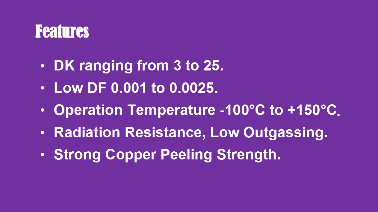
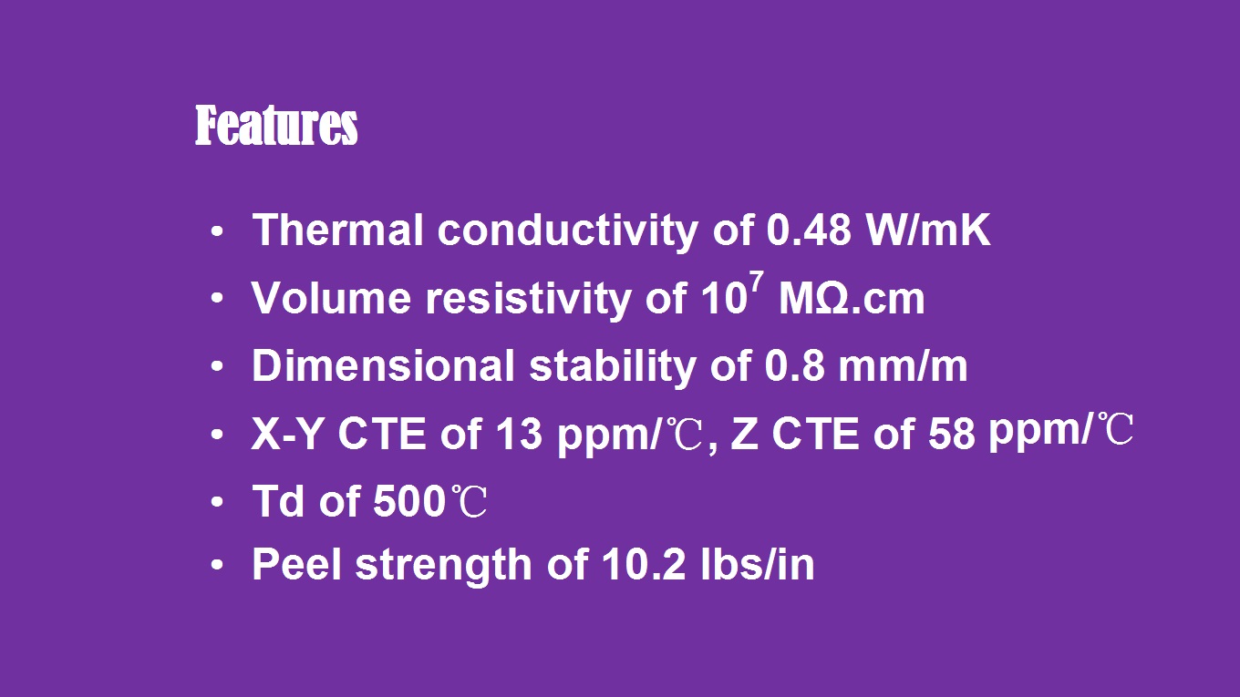
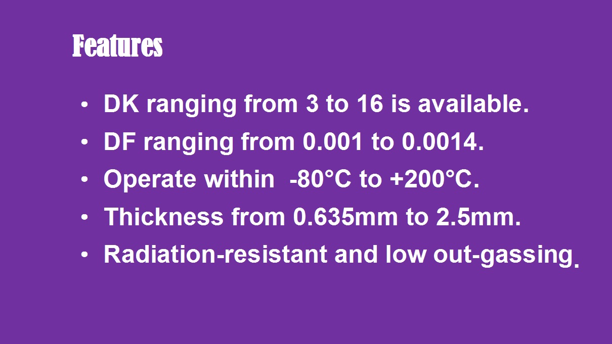
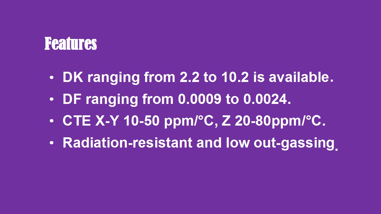
TC350 Features


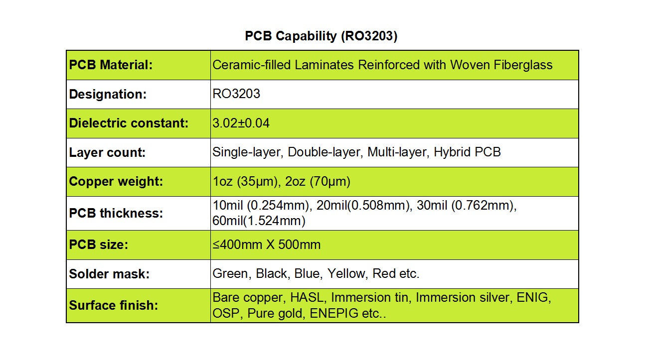
PCB Manufacturing Capabilities for Rogers TC350

As a reliable PCB supplier, we offer advanced fabrication services tailored to Rogers TC350 laminates, ensuring high-quality, high-performance boards for your RF and microwave applications.


1. Board Configurations

Single-sided, double-sided, and multi-layer PCBs

Hybrid constructions (combining Rogers TC350 with other high-frequency materials like RO4003C or FR4)


2. Copper Weight Options

1 oz (35 µm)–Standard thickness for signal integrity

2 oz (70 µm)–Enhanced current-carrying capacity for power applications


3. PCB Thickness & Size

Available thicknesses: 10 mil, 20 mil, 25 mil, 60 mil, 125 mil

Maximum PCB size: 400 mm×500 mm


4. Solder Mask & Surface Finishes

Solder mask colors: Green, black, blue, yellow, red

Surface finishes: Bare copper, HASL, ENIG, OSP, immersion silver, immersion tin, ENEPIG, pure gold


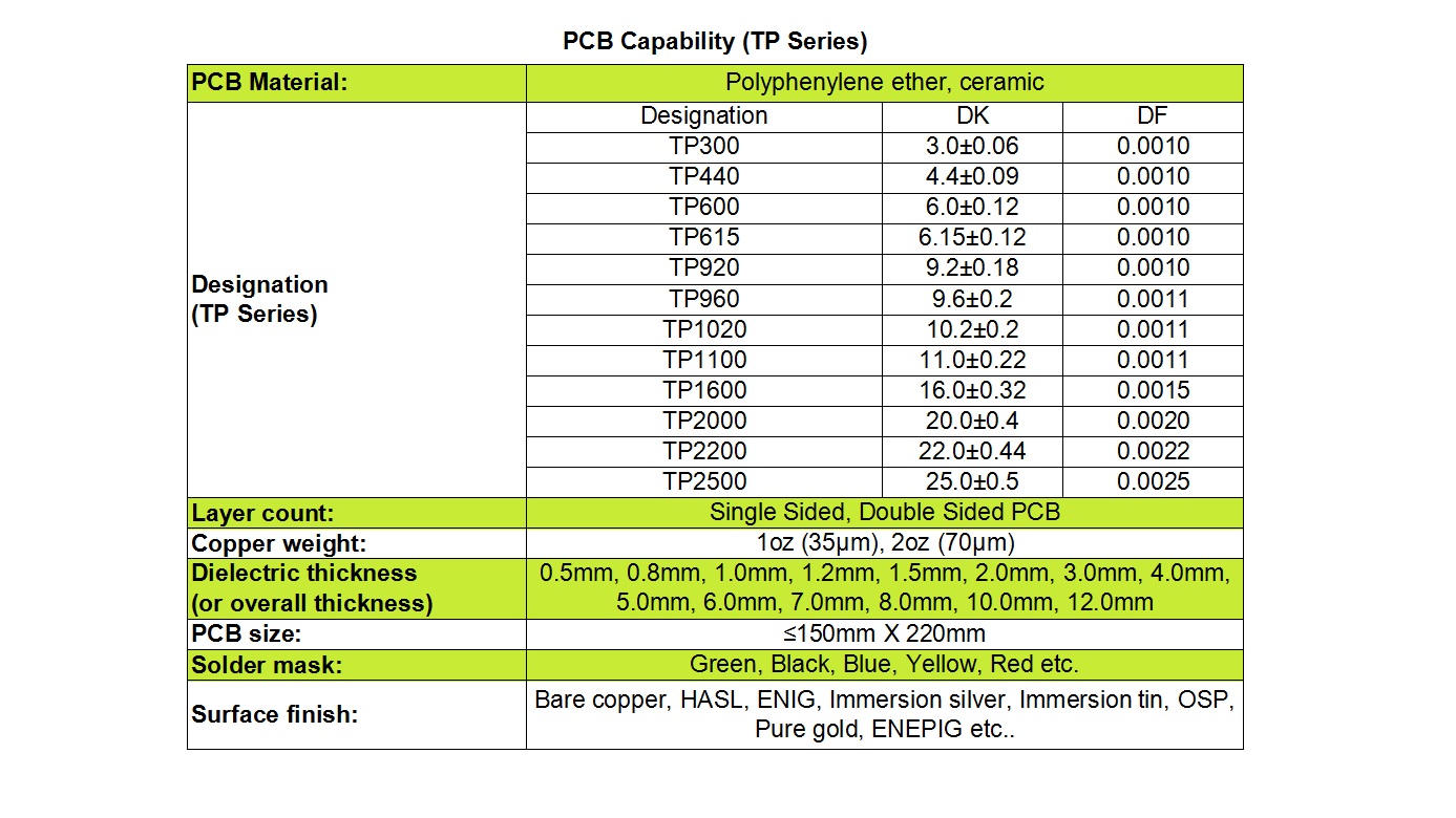
TC350 PCB Capability


Applications of Rogers TC350 PCB

Due to its exceptional thermal and electrical properties, Rogers TC350 is widely used in high-frequency and high-power applications, including:


  • Power amplifiers (for 5G, radar, and satellite communications)
  • RF filters & couplers
  • Tower-mounted amplifiers (TMA) & boosters (TMB)
  • Microwave combiners & power dividers
  • Military & aerospace electronics
  • Automotive radar & ADAS systems


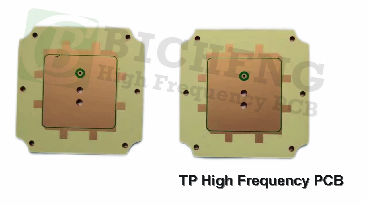
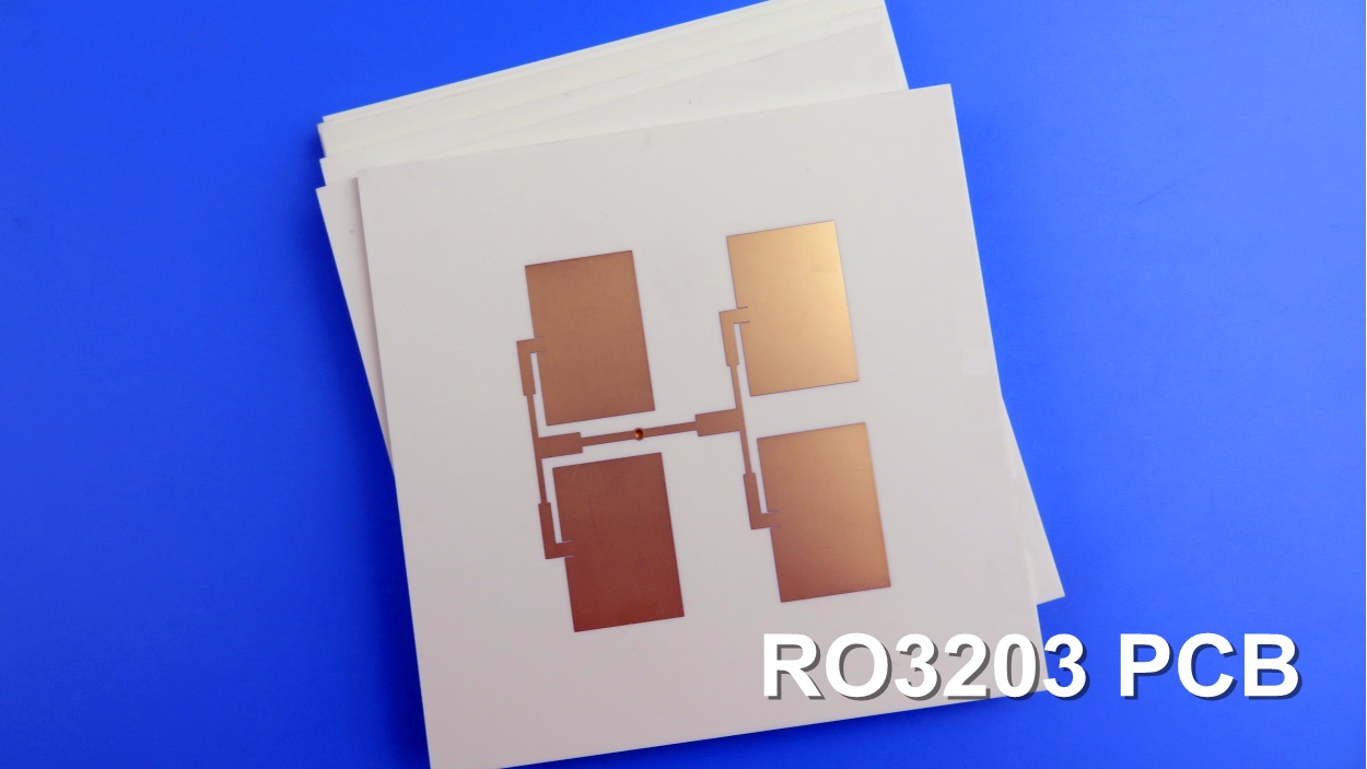
 Rogers TC350 boards


Conclusion

TC350 high frequency PCB is a high-performance solution for demanding RF and microwave applications, offering superior thermal management, stable electrical properties, and excellent reliability. Whether you need high-power amplifiers, low-loss filters, or high-efficiency antennas, TC350 laminates provide the thermal and electrical stability required for optimal performance.


As an experienced PCB supplier, we specialize in producing high-quality Rogers TC350 boards tailored to your specifications. Contact us today to discuss your project requirements and leverage the benefits of this advanced material for your next high-frequency design!


Why Choose RO4350B Over PTFE for Cost-Effective High-Frequency PCBs?


Introduction to RO4350B High Frequency PCB

In the realm of high-frequency printed circuit boards (PCBs),Rogers RO4350B stands out as a high-performance material engineered for demanding RF and microwave applications. This advanced laminate combines a proprietary blend of woven glass-reinforced hydrocarbon/ceramic materials, delivering electrical performance on par with PTFE/woven glass while maintaining the manufacturability benefits of traditional epoxy/glass laminates.


RO4350B laminates provide exceptional control over dielectric constant (Dk) while ensuring minimal signal loss. Unlike PTFE-based materials, which often require specialized handling and through-hole treatments, Rogers 4350B can be processed using standard FR-4 fabrication techniques, significantly reducing production costs and lead times. Additionally, these materials meet the stringent UL 94 V-0 flammability rating, making them ideal for high-power RF designs and active electronic devices where reliability is critical.


Key Features of RO4350B High Frequency PCB


1. Low Dielectric Constant for Enhanced Signal Integrity

RO4350B laminates exhibit a stable dielectric constant (Dk) of 3.50 at 10 GHz, ensuring consistent signal propagation in high-frequency circuits. A low Dk is essential for minimizing signal delay and distortion, making RO4350B an excellent choice for high-speed digital and RF applications.


2. Ultra-Low Dissipation Factor for Minimal Signal Loss

With a dissipation factor (Df) of just 0.0017 at 10 GHz, RO4350B PCB ssignificantly reduce signal attenuation, preserving signal integrity even in high-frequency environments. This low-loss characteristic is crucial for applications such as 5G communications, radar systems, and satellite technology.


3. Excellent Thermal and Dimensional Stability

RO4350B offers outstanding dimensional stability, with a Z-axis coefficient of thermal expansion (CTE) of 24 ppm/°C, closely matching that of copper. This alignment prevents delamination and ensures reliable performance under thermal stress. Additionally, the material boasts a glass transition temperature (Tg) exceeding 280°C (536°F), enabling it to withstand high-temperature assembly processes such as lead-free soldering without warping or degradation.


4. Superior Mechanical and Environmental Resistance

Engineered for durability, RO4350B substrate PCBs resist moisture absorption and environmental factors that could compromise performance. Their robust construction ensures long-term reliability in harsh operating conditions, making them suitable for aerospace, defense, and automotive applications.


RO4350B Features 


PCB Manufacturing Capabilities for RO4350B

We provide a comprehensive range of fabrication options to meet diverse design requirements:


1. Board Configurations

Single-sided, double-sided, and multi-layer PCBs

Hybrid constructions combining RO4350B with other high-frequency or standard materials


2. Available Thickness Options

Standard thicknesses: 10 mil, 20 mil, 30 mil, 60 mil

Custom thicknesses: 4 mil, 6.6 mil, 13.3 mil, 16.6 mil, and others upon request


3. Copper Weight and Board Size

Finished copper options: 1oz or 2oz

Maximum PCB dimensions: 400mm x 500mm


4. Solder Mask and Surface Finishes

Solder mask colors: Green, black, red, yellow, and more

Surface finishes: Bare copper, HASL, immersion gold (ENIG), immersion silver, immersion tin, OSP, ENEPIG, and pure gold plating


RO4350B pcb capability 


Applications of RO4350B High Frequency PCBs

RO4350B high frequency PCBs are widely used in industries where high-frequency performance and reliability are non-negotiable. Some key applications include:


5G and mmWave Communication Systems–Ensures low signal loss in high-frequency transmission lines and antennas.


Aerospace and Defense Electronics–Provides stable performance in radar systems, avionics, and satellite communications.


Automotive Radar and ADAS (Advanced Driver Assistance Systems)–Supports high-frequency signal processing for collision avoidance and autonomous driving.


Medical RF Devices–Used in high-precision diagnostic and therapeutic equipment.


High-Power RF Amplifiers and Base Station Antennas–Delivers efficient power handling with minimal insertion loss.


RO4350B high frequency PCBs


Why Choose Us for Your RO4350B PCB Needs?

As a trusted PCB supplier, we combine advanced fabrication techniques, stringent quality control, and deep expertise in high-frequency materials to deliver Rogers RO4350B PCBs that meet the highest industry standards. Whether you require prototypes or high-volume production, we provide competitive pricing, fast turnaround times, and exceptional technical support to ensure your project’s success.


Contact us today to discuss your RO4350B PCB requirements and discover how we can help optimize your high-frequency designs for superior performance and reliability!


We are excited to announce that CIQTEKin collaboration with our UK distributor SciMed, will be exhibiting at the 10th European Federation of EPR (EFEPR) Summer School.


>> Date: August 31 – September 6, 2025
>> Location: University of Manchester, United Kingdom


This prestigious week-long event brings together up to 130 emerging Electron Paramagnetic Resonance ( EPR) spectroscopists, supported by a rich program of lectures, hands-on tutorials, practical demonstrations, and poster sessions delivered by leading experts from across Europe and beyond.

The EFEPR Summer School provides an exceptional opportunity for participants to deepen their understanding of EPR theory and its applications, engage in practical laboratory sessions, and connect with peers in the EPR community.


We will bring a live CIQTEK EPR instrument to the event, offering attendees the chance to see and experience our system in action. Whether you're a student or seasoned researcher, we invite you to stop by and discover how CIQTEK EPR solutions can support your work.


We look forward to meeting you in Manchester!

CIQTEK and SciMed to Exhibit at 10th EFEPR Summer School 2025, UK

CIQTEK field emission scanning electron microscope meets world-leading standards in all major specifications, offers a long warranty, and provides highly responsive after-sales support. After two years of use, we are confident that the system delivers lasting scientific value and performance at a highly competitive cost.”
— Dr. Zhencheng Su, Senior Engineer and head of the Molecular Biology Lab, Institute of Applied Ecology, Chinese Academy of Sciences


In Shenyang, Liaoning Province, stands a prestigious research institute with a history dating back to 1954. Over the past 70 years, it has grown into a national powerhouse in ecological research — the Institute of Applied Ecology (IAE), part of the Chinese Academy of Sciences (CAS). The institute focuses on forest ecology, soil ecology, and pollution ecology, making significant contributions to the national ecological civilization.

In 2023, as the institute approached a critical phase of equipment upgrades, it made a strategic decision that would not only reshape its research workflow but also establish a model case for the application of CIQTEK scanning electron microscopes (SEM) in the field of biology.


IAE CAS: Advancing Ecological Civilization with Science

IAE CAS operates three major research centers in forestry, agriculture, and environmental studies. Dr. Su recalls the development of the institute's shared technical service platforms.

Established in 2002, the Molecular Biology Laboratory is a core facility within IAE's Public Technology Center. Over the past two decades, the lab has acquired more than 100 sets of large-scale general-purpose instruments, valued at over 7 million USD. It supports internal research needs and also serves the public by offering testing services, including isotopic and tracer analysis, biological structure identification, trace element ecological analysis, and molecular biology services.


Affordable Brilliance: CIQTEK SEMs Deliver Beyond Expectations

For biological research, scanning electron microscopy is indispensable. “Our electron microscopy lab handles a wide range of biological samples, including plant and animal tissues, microbial cells, fungal spores, and viruses, as well as material samples like mineral particles, microplastics, and biochar,” Dr. Su explained.

The FE-SEM is capable of producing highly detailed 3D surface structures of solid-state samples. With a scanning transmission detector, it can also reveal internal structures of thin samples. In addition, the built-in high-performance EDS (energy-dispersive X-ray spectroscopy) enables qualitative and semi-quantitative elemental analysis on sample surfaces.

By 2023, their previous SEMs (an environmental SEM and a benchtop SEM) could no longer meet the growing demand for higher resolution and imaging precision. A new FE-SEM became necessary.

“After comprehensive evaluation and expert reviews, CIQTEK SEM5000 Series was selected through a competitive public bidding process,” Dr. Su recalled. “Its technical specifications align with global standards, the extended warranty is reassuring, and the after-sales service has been extremely responsive. After two years of use, we are very satisfied with its truly excellent value.”

CIQTEK SEM Microscopy at IAE, CASCIQTEK SEM Microscopy at IAE, CAS


Field-Tested Excellence: CIQTEK SEMs Stand Out

Lee Xu, a key operator of the SEM5000 at the institute, is particularly impressed with the CIQTEK SEM5000's performance.

“The SEM5000 allows us to observe a wide variety of biological and material samples at magnifications ranging from 2,000x to 100,000x, and the image quality remains excellent throughout that range,” Lee noted.

One impressive feature is the user-friendly software.

“The interface is intuitive and easy to use. One of my favorite features is automatic brightness and contrast adjustment. It speeds up image acquisition and ensures consistent lighting in captured images.”

The after-sales support stands out.

“CIQTEK’s SEM engineers regularly check in on the instrument status and provide timely maintenance. Any issues we’ve encountered have been resolved quickly and professionally.”

The paired EDS system also performs reliably.

“It enables both qualitative and quantitative analysis of elemental composition on the sample surface. Point analysis is the most commonly used approach, allowing the detection of elements at specific spots or micro-areas, which is ideal for studying localized chemical properties. Line analysis helps map the distribution of selected elements along a defined path, revealing concentration gradients in materials.”

Since its installation, the CIQTEK SEM5000 has played a vital role in the lab’s scientific output.

“Over the past year and a half, we’ve analyzed a large number of biological and material samples,” said Lee. “The data and images generated have been used in theses, publications, and ongoing research.”


Notable Publications Utilizing CIQTEK SEM5000 Data:

  • "Acetochlor accelerates the aging of plastic film microplastics in soil by altering the plastisphere microbiota", published in the Journal of Hazardous Materials.

  • "Four new species of Trichoderma from subtropical forests in Southwest China", published in the Journal of Fungi.

IAE, CAS Team Analyzing with the CIQTEK SEM MicroscopyIAE, CAS Team Analyzing with the CIQTEK SEM Microscopy

We are excited to announce that CIQTEK will exhibit at JASIS 2025, one of the largest exhibitions in Asia for analytical and scientific instruments. We warmly invite you to visit us at Booth 7B-407 to explore our latest innovations and connect with our expert team.

  • Date: September 3–5, 2025
  • Location: Makuhari Messe International Exhibition Hall, Chiba, Japan
  • CIQTEK Booth: 7B-407

At this year’s show, CIQTEK will highlight a range of cutting-edge technologies across multiple categories, including:

Electron Microscopy (SEM, FIB-SEM, TEM)

Experience the performance of CIQTEK’s high-resolution scanning electron microscopes (SEM) and focused ion beam FIB-SEM, designed to support advanced research in materials science, life sciences, semiconductors, and more.


Electron Paramagnetic Resonance (EPR) Spectrometer

Discover our growing EPR product portfolio, including floor-standing/benchtop EPR, pulse/CW EPR, widely used in chemistry, materials, catalysis, and biological research.


Surface Area and Porosity Analysis

CIQTEK will also showcase its BET analyzers and related instruments for surface area, pore size, and gas adsorption characterization, which are critical tools in fields like pharmaceuticals, catalysts, and nanomaterials.


See you at Booth 7B-407

Join us to discover how CIQTEK is advancing the future of scientific instrumentation!

Discover CIQTEK Flagship Technologies at JASIS 2025, Booth 7B-407

When choosing a high-speed scanning electron microscope (SEM) for a research lab, it's not just about magnification or resolution anymore. Modern research demands faster, smarter, and more flexible imaging solutions. Whether you’re working in materials science, life sciences, nanotechnology, or additive manufacturing, the right SEM can dramatically accelerate your workflow and elevate your results.

Here are the top 5 features to consider when evaluating high-speed SEMs for your research:


1. Fast Scanning with High Image Quality

Speed is crucial in high-throughput environments, but it shouldn’t come at the expense of image quality. Look for an SEM with fast scan capabilities, including:

  • High scanning speeds without distortion

  • Real-time image rendering

  • Flexible dwell time control

This enables researchers to image more samples in less time while maintaining the high-resolution detail necessary for in-depth analysis. The best fast SEM imaging systems will strike this balance perfectly.


2. Low Voltage Imaging Capabilities

Delicate samples, especially biological, polymer, or nanostructured materials, are sensitive to beam damage. A top-tier SEM should support:

  • Stable imaging at low accelerating voltages (e.g., 0.2–5 kV)

  • Surface-sensitive detail without conductive coating

  • Reduced sample charging and artifacts

Choosing a low-voltage SEM helps expand your imaging possibilities and protect valuable specimens.


3. Automated Functions for Reproducibility & Efficiency

Automation isn’t just convenient. It transforms productivity. Leading-edge SEMs now offer:

  • Auto focus, auto stigmation, and auto contrast/brightness

  • Automated stage navigation, area mapping, and image stitching

  • Pre-programmed imaging workflows for routine analysis

A truly automated SEM reduces user variability and supports reproducible results across multiple users or shifts.


4. Flexible Data Export and Smart Analysis Tools

Today’s labs need more than just images; they need actionable data. The right SEM for research labs should provide:

  • Easy data export in multiple formats (TIFF, JPEG, raw, etc.)

  • Compatible interfaces with third-party analysis software

  • Support for real-time EDS or 3D image reconstruction

An SEM’s data management features are often overlooked, but they are crucial for streamlining post-imaging workflows and collaborations.


5. Exceptional Speed and Value: Why Labs Are Choosing CIQTEK HEM6000

For research labs seeking the best SEM for high-speed imaging, CIQTEK HEM6000 delivers a compelling balance of performance, versatility, and affordability:

  • High-speed SEM imaging with distortion-free results

  • Low-voltage SEM capabilities down to 200 V for sensitive or non-conductive samples

  • Smart automation features like auto focus, stigmation, and stage navigation

  • 5-axis motorized stage and large sample chamber for flexible workflows

  • High-resolution output across a wide voltage range

  • User-friendly interface and intuitive controls, ideal for both experts and new users

Whether you're upgrading your current system or setting up a new lab, CIQTEK HEM6000 stands out as a high-speed SEM that accelerates discovery without compromising your budget.

ciqtek High Speed SEM


Selecting the right high-speed SEM involves more than comparing datasheets. It’s about finding a system that:

  • Matches your research goals

  • Speeds up your imaging workflow

  • Supports reproducibility and collaboration

  • Provides long-term value

By focusing on the five key features above and exploring cutting-edge options like the CIQTEK HEM6000, you’re investing in better data, faster insights, and more impactful research.


Ready to Accelerate Your Research with CIQTEK HEM6000?


Contact CIQTEK today to learn how our high-speed SEM solutions can help your lab achieve fast, reliable, and cost-effective imaging.

WAIN “High-Voltage Connector Series for Special Vehicles” is a high-performance, compact alloy-shell interconnect solution designed for construction machinery, commercial vehicles, and other special-purpose vehicles.

This solution features a unique design and advanced manufacturing process, delivering electrical ratings of up to 1500V DC and 500A Max. It is equipped with IP67/IP69K level protection and 360° electromagnetic shielding for optimal durability and reliability.

Additionally, it offers multiple keying options, both angled and straight cable outlet configurations, and supports up to three contact positions, accommodating cable sizes ranging from 2.5mm² to 120mm².

This connector series is widely used in the power distribution systems of various vehicles, including automobiles, trucks, buses, agricultural vehicles, construction vehicles, and off-road vehicles, as well as in the power supply applications of agricultural, construction, and off-road machinery. 


In the new energy sector, WAIN primarily provides essential services to electric vehicle manufacturers and supports traditional construction machinery companies transitioning toward new energy solutions. WAIN has successfully developed a comprehensive range of products compliant with GB/T 20234.1 and IEC 62196.2 standards, including GB/T AC/DC charging sockets, GB/T AC charging guns, and Type 2 charging guns and sockets. Particularly notable is the PCBA quick-change terminal version of the GB/T DC charging socket, which significantly enhances efficiency and reduces costs in wiring harness applications and maintenance.

In addition to supporting mass production for customers in the construction machinery and electric vehicle sectors, WAIN proactively aligns with industry trends in electric vehicle technology, especially battery-swapping solutions. The company continuously develops innovative products tailored to customer needs, providing diverse options to enhance battery-swapping systems.

CIQTEK successfully concluded a dynamic and rewarding week at Microscopy & Microanalysis 2025 (M&M 2025), one of the most influential events in the global microscopy community. This marks another important milestone as we continue to expand our presence in the North American electron microscopy market.


CIQTEK at M&M 2025: Advancing Our North American Electron Microscopy Journey


At the booth, our team engaged with a wide range of researchers and professionals from materials science, life science, and beyond. We showcased our latest innovations in high-performance field emission scanning electron microscopy (FESEM), with a focus on imaging speed, resolution, and user-friendly operation. The strong interest and positive feedback we received on-site reaffirmed the value of our technologies to the scientific community.

A key highlight of the event was our well-attended Vendor Tutorial, featuring CIQTEK electron microscopy expert Mr. Luke Ren. His presentation on high-speed FESEM (HEM) imaging sparked insightful discussions and active engagement from the audience. We were excited to see the high level of interest, and we sincerely thank everyone who participated and contributed to the success of this session.


CIQTEK at M&M 2025: Advancing Our North American Electron Microscopy Journey


We also extend our heartfelt thanks to our trusted U.S. distributor, JH Technologies, for their outstanding support throughout the event. Their professionalism and dedication played a crucial role in helping us connect with more users and partners nationwide. Together, we are building a stronger foundation for CIQTEK's long-term growth in North America.

M&M 2025 was not just a trade show; it was a meaningful step forward in our journey to bring cutting-edge electron microscopy solutions to more scientists and institutions. We are energized by the conversations and inspired by the collaborations, and we are already looking ahead to future opportunities.


We look forward to seeing you at M&M 2026 in Milwaukee!

Sodium-ion batteries (SIBs) are attracting attention as a cost-effective alternative to lithium-ion batteries, thanks to the abundant sodium content in Earth’s crust (2.6% vs. 0.0065% for lithium). Despite this, SIBs still lag in energy density, highlighting the need for high-capacity electrode materials. Hard carbon is a strong candidate for SIB anodes due to its low sodium storage potential and high capacity. However, factors like graphite microdomain distribution, closed pores, and defect concentration significantly impact initial Coulombic efficiency (ICE) and stability. Modification strategies face limits. Heteroatom doping can raise capacity but reduce ICE. Traditional CVD helps form closed pores but suffers from slow methane decomposition, long cycles, and defect buildup.


AFM Publication: CIQTEK SEM Aids in Hard Carbon Morphology Study

Professor Yan Yu’s team at the University of Science and Technology of China (USTC) utilized the CIQTEK Scanning Electron Microscope (SEM) to investigate the morphology of various hard carbon materials. The team developed a catalyst-assisted chemical vapor deposition (CVD) method to promote CH₄ decomposition and regulate the microstructure of hard carbon. Transition metal catalysts such as Fe, Co, and Ni effectively lowered the energy barrier for CH₄ decomposition, thereby improving efficiency and reducing deposition time.

However, Co and Ni tended to cause excessive graphitization of the deposited carbon, forming elongated graphite-like structures in both lateral and thickness directions, which hindered sodium-ion storage and transport. In contrast, Fe facilitated appropriate carbon rearrangement, resulting in an optimized microstructure with fewer defects and well-developed graphite domains. This optimization reduced irreversible sodium storage, enhanced initial Coulombic efficiency (ICE), and increased the availability of reversible Na⁺ storage sites.

As a result, the optimized hard carbon sample (HC-2) achieved an impressive reversible capacity of 457 mAh g⁻¹ and a high ICE of 90.6%. Moreover, in-situ X-ray diffraction (XRD) and in-situ Raman spectroscopy confirmed a sodium storage mechanism based on adsorption, intercalation, and pore filling. The study was published in Advanced Functional Materials under the title:
Catalyst-Assisted Chemical Vapor Deposition Engineering of Hard Carbon with Abundant Closed Pores for High-Performance Sodium-Ion Batteries.


AFM Publication: CIQTEK SEM Aids in Hard Carbon Morphology Study


As illustrated in Figure 1a, the hard carbon was synthesized via a catalyst-assisted chemical vapor deposition (CVD) method using commercial porous carbon as the precursor and methane (CH₄) as the feed gas. Figure 1d shows the adsorption energies of CH₄ and its dehydrogenated intermediates on metal catalysts (Fe, Co, Ni) and porous carbon surfaces, indicating that the introduction of metal catalysts lowers the energy barrier for CH₄ decomposition, with Fe being the most effective in promoting the breakdown of CH₄ and its intermediates.

High-resolution TEM (HRTEM) images under different catalyst conditions (Figures 1e–h) reveal that:

  • Without a catalyst, the hard carbon exhibits a highly disordered structure rich in defects.

  • With Fe as the catalyst, the resulting hard carbon features short-range ordered graphite-like microcrystals and closed pores embedded between graphite domains.

  • Co promotes the expansion of graphite domains and increases the number of graphite layers.

  • Ni leads to a graphitic structure and even the formation of carbon nanotubes, which, despite their high order, are unfavorable for sodium-ion storage and transport.


AFM Publication: CIQTEK SEM Aids in Hard Carbon Morphology Study


Figure 2 presents the structural characterization results of hard carbon materials prepared with varying concentrations of FeCl₃. The XRD patterns (Figure 2a) and Raman spectra (Figure 2b) indicate that as the FeCl₃ concentration in the impregnation solution increases, the graphite interlayer spacing gradually decreases (from 0.386 nm to 0.370 nm), the defect ratio (ID/IG) decreases, and the lateral crystallite size (La) increases. These changes confirm that Fe catalyzes the rearrangement of carbon atoms, enhancing the degree of graphitization.

X-ray photoelectron spectroscopy (XPS) results (Figures 2c and 2e) show that with increasing Fe catalyst concentration, the proportion of sp²-hybridized carbon in hard carbon increases, further indicating improved graphitization. At the same time, the oxygen content in the hard carbon decreases, which may be attributed to hydrogen (H₂) generated from CH₄ decomposition consuming oxygen during carbonization, thereby reducing surface oxygen-related defects.

Small-angle X-ray scattering (SAXS) analysis (Figure 2f) reveals average closed-pore diameters of 0.76, 0.83, 0.90, 0.79, and 0.78 nm, respectively. Larger closed pores are beneficial for stabilizing sodium clusters and improving Na⁺ transport kinetics.

HRTEM images (Figures 2g–i) show small graphite domains at low Fe loading, while excessive catalyst loading leads to long-range ordered structures with narrower interlayer spacing, which can hinder Na⁺ transport.


AFM Publication: CIQTEK SEM Aids in Hard Carbon Morphology Study


Figure 3 shows the effect of different Fe catalyst loadings on the electrochemical performance of hard carbon materials. Galvanostatic charge–discharge tests (Figure 3a) reveal that as the concentration of FeCl₃ in the impregnation solution increases, HC-2 (0.02 M FeCl₃) exhibits the best performance, with a reversible capacity of 457 mAh g⁻¹ and a high initial Coulombic efficiency (ICE) of 90.6%. The low-voltage plateau accounts for a significant portion of the capacity (around 350 mAh g⁻¹), indicating the advantage of closed pores in sodium storage.

Excessive catalyst loading (e.g., HC-4) leads to a decrease in capacity (377 mAh g⁻¹) due to the over-ordering of carbon layers, highlighting the need to balance graphite domain growth and sodium-ion transport pathways. After 100 cycles at a current density of 0.5 A g⁻¹, the capacity remains at 388 mAh g⁻¹, demonstrating that larger closed pores enhance the stability of Na clusters and improve Na⁺ transport kinetics.


AFM Publication: CIQTEK SEM Aids in Hard Carbon Morphology Study


Figure 4 shows the SEI structure on different hard carbon surfaces: (a) and (b) depict the depth profiles and distributions of NaF⁻, P, and CH₂ species in opt-HC and HC-2, respectively. (c) and (d) present TEM images of opt-HC and HC-2 after 10 cycles at 30 mA g⁻¹. (e) and (f) display the XPS spectra of opt-HC and HC-2 after 10 cycles at 30 mA g⁻¹. (g) shows the HRTEM image of HC-2 after 10 cycles at 30 mA g⁻¹. EPMA mapping images of the electrode cross-sections for (h) opt-HC and (i) HC-2 are shown after the first cycle.


AFM Publication: CIQTEK SEM Aids in Hard Carbon Morphology Study


As shown in Figure 5, the GITT curves (Figure 5a) reveal that the Na⁺ diffusion coefficient (DNa⁺) of HC-2 is higher than that of opt-HC, indicating that HC-2 exhibits faster kinetics and enables quicker Na⁺ diffusion.

The in situ Raman spectra (Figure 5b) show that during discharge from open-circuit voltage to approximately 0.7 V, the D-band gradually broadens while the G-band remains relatively unchanged, suggesting that sodium storage at this stage is dominated by surface adsorption. As discharge proceeds further, the D-band intensity weakens and the G-band redshifts, indicating that Na⁺ begins to intercalate into graphene layers. After reaching the plateau near 0.05 V, the G-band stabilizes, implying that Na⁺ fills into the closed pores.

In the in situ XRD patterns (Figure 5c), the (002) peak intensity of HC-2 significantly decreases at lower angles during discharge, confirming Na⁺ intercalation between graphene layers. Compared to opt-HC, the (002) peak shift in HC-2 is more pronounced, indicating a greater extent of Na⁺ intercalation into the carbon layers, contributing to its higher capacity.

Together, Figures 5b and 5c illustrate that the sodium storage mechanism involves: (1) Na⁺ adsorption, (2) Na⁺ interlayer adsorption/intercalation, and (3) Na⁺ pore filling and clustering.


AFM Publication: CIQTEK SEM Aids in Hard Carbon Morphology Study


Figure 6 illustrates the electrochemical performance of a full cell assembled using the HC-2 anode and an O3-type NaNi₁/₃Fe₁/₃Mn₁/₃O₂ cathode. The cell demonstrates excellent rate capability and long-term cycling stability under various current densities, confirming the potential of the HC-2 anode for practical battery applications.


Professor Yu Yan’s team proposed a novel catalyst-assisted chemical vapor deposition (CA-CVD) method that enables the precise synthesis of hard carbon anodes featuring abundant closed pores, well-developed graphitic domains, and controllable defects. The optimized HC-2 anode exhibits a high reversible capacity of 457 mAh g⁻¹ and an impressive initial Coulombic efficiency of 90.6%. When paired with an O3-type layered cathode in a soft-packed full cell, the battery retains 83% of its capacity after 100 cycles, maintaining a reversible capacity above 400 mAh g⁻¹.

This method not only offers a new route for the controlled fabrication of high-capacity and high-efficiency hard carbon anodes but also provides mechanistic insights into sodium storage behavior, supporting further optimization of material systems. It holds significant promise for advancing high-energy-density sodium-ion battery (SIB) technologies toward practical applications.