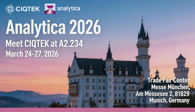
CIQTEK Exhibits at SMTA and TSM 2026, Expands U.S. SEM Presence
2026 is a fresh start for CIQTEK Electron Microscope USA operations.
This year, we officially formed a dedicated CIQTEK US team. That means more local presence, faster response, and closer communication with customers across the country.
And we are not staying behind a desk.
Our U.S. team, together with our official local distributor, JH Technologies, recently participated in the SMTA Wafer-Level Packaging Symposium 2026 and the 60th Anniversary Meeting of the Texas Society for Microscopy (TSM).
Supporting Advanced Packaging at SMTA 2026
At the SMTA Wafer-Level Packaging Symposium in San Francisco, we connected with engineers and technical experts working in advanced semiconductor packaging.
As devices continue to shrink, inspection and defect analysis become more demanding. Reliable SEM solutions USA customers can trust are more important than ever. We had open, practical conversations about real challenges in wafer-level packaging. Topics included imaging resolution, surface characterization, and process optimization.
These discussions help us better understand how the CIQTEK electron microscope can support advanced manufacturing and research applications.
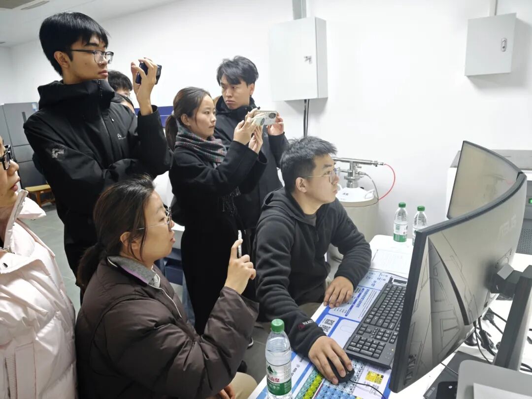
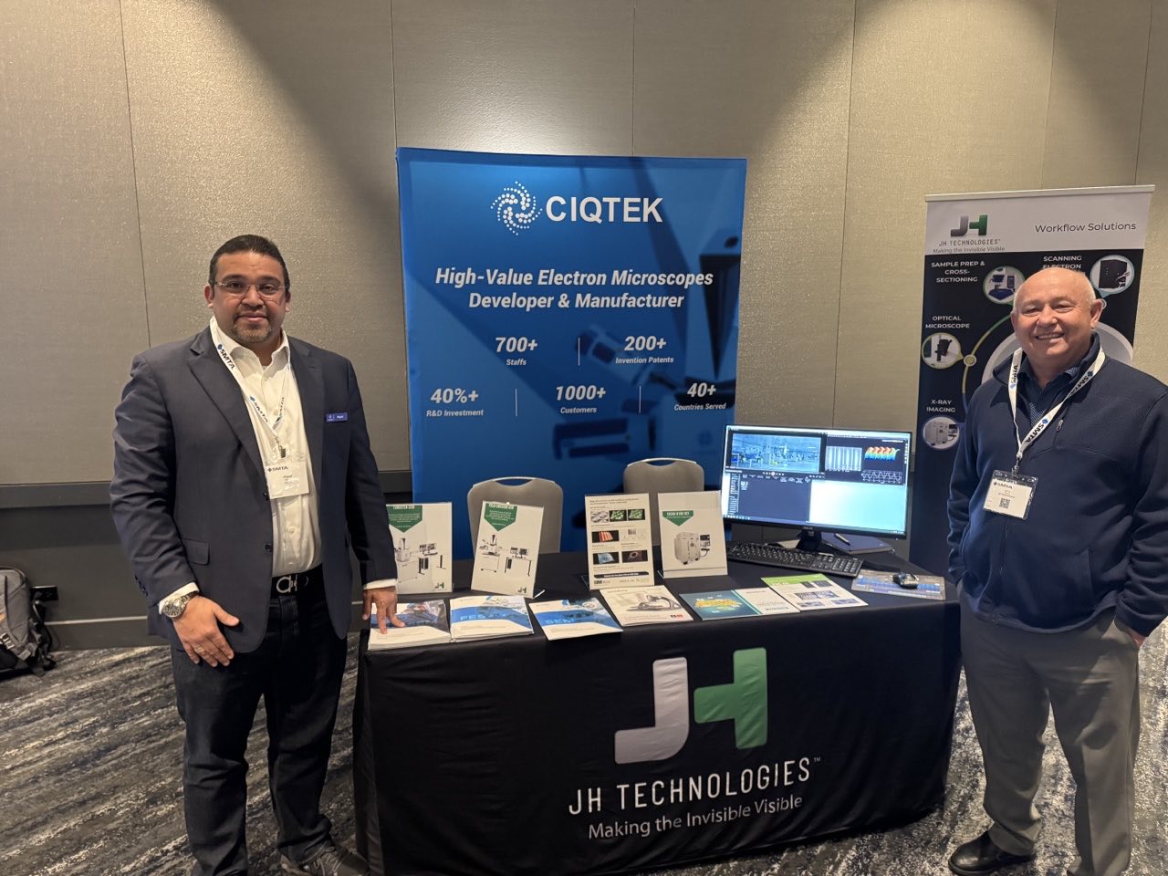 CIQTEK and JH Technologies at the SMTA 2026
TSM 2026: The Start of Regional Engagement
The 60th Anniversary Meeting of the Texas Society for Microscopy was especially meaningful.
Unlike large national exhibitions, microscopy society events in the USA, such as TSM, allow for closer, more personal conversations. We met researchers, lab managers, and industry professionals from materials science, life sciences, and industrial labs.
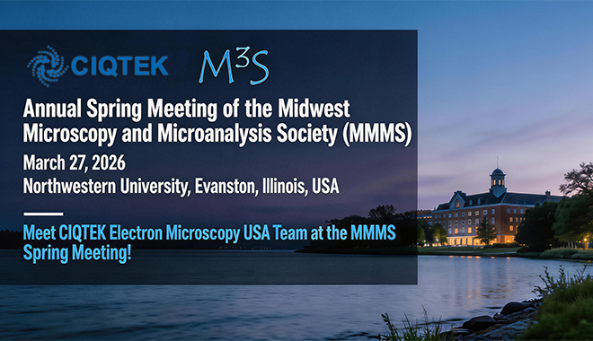
For CIQTEK, TSM 2026 is the starting point of a broader plan. Our new CIQTEK US team will continue visiting regional microscopy societies across the country. We believe real relationships are built face-to-face.
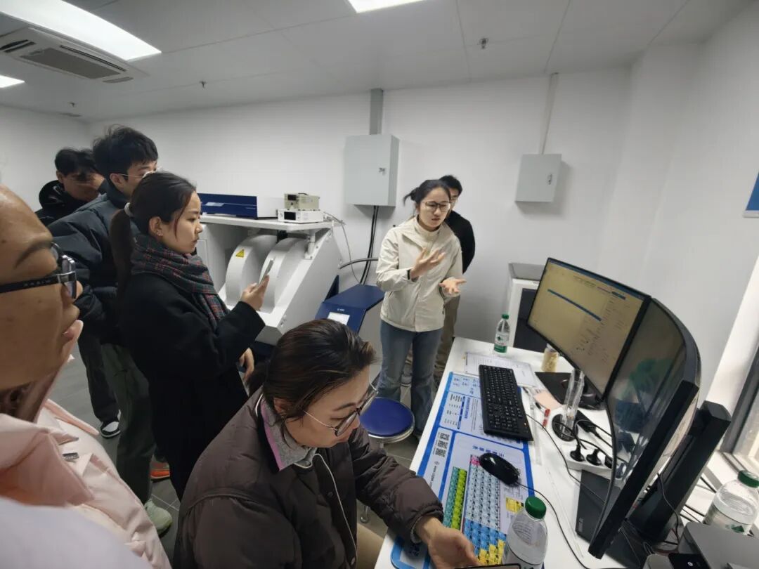
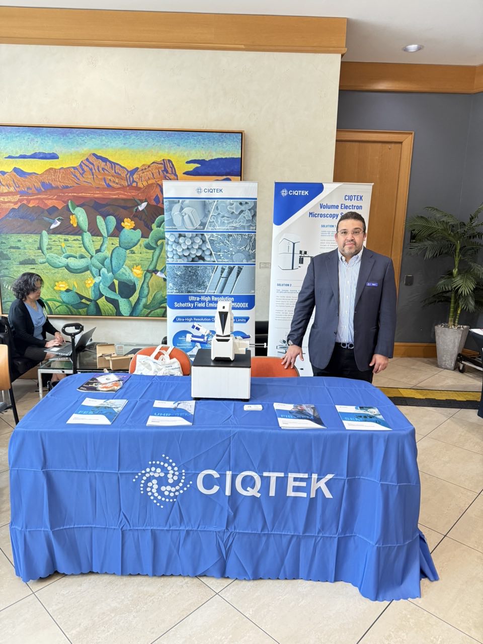 CIQTEK at the TSM 2026
2026 Is Just the Beginning
The launch of our CIQTEK US team marks a new phase for CIQTEK electron microscope USA development.
We are investing in local support.
We are building stronger partnerships.
We are becoming part of the American microscopy ecosystem.
More regional visits are coming.
More technical exchanges are ahead.
2026 is not just another year. It is the year CIQTEK steps closer to the U.S. microscopy community.
And this is only the beginning.
 A group photo of the CIQTEK mascot, Matteo from the MS lab, and the Winter Olympics mascot