How Does RO3203 Laminate Deliver Superior Electrical and Mechanical Performance Cost-Effectively?


Introduction

In the rapidly advancing world of wireless communication and high-speed electronics, the choice of printed circuit board (PCB) substrate material is paramount. For engineers and designers working on cutting-edge RF, microwave, and millimeter-wave applications, achieving optimal electrical performance without compromising mechanical reliability or budget is a constant challenge. Enter RO3203 high-frequency circuit materials, a superior class of laminates engineered to meet these exacting demands. As a strategic extension of the renowned RO3000 PCB series, Rogers RO3203 stands out by offering an exceptional balance of electrical properties, enhanced mechanical stability, and cost-effectiveness. This blog post provides a comprehensive exploration of the RO3203 material, its key characteristics, our advanced PCB fabrication capabilities, and its diverse application fields, illustrating why it is a premier choice for high-frequency designs.


The Properties of RO3203 Material

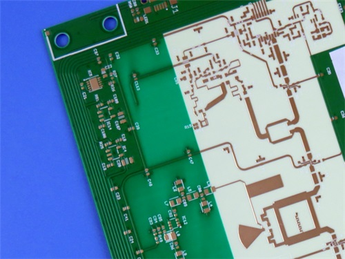
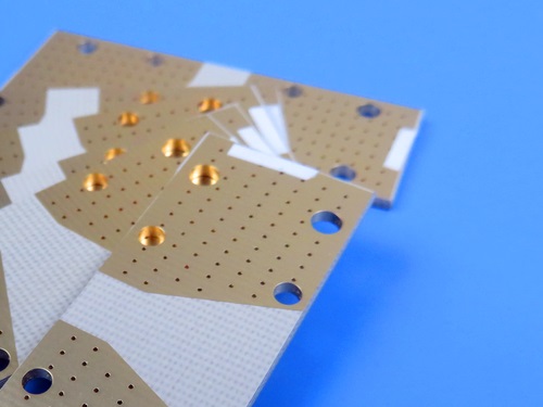
Rogers 3203 PCB is constructed as a ceramic-filled polytetrafluoroethylene (PTFE) composite laminate, reinforced with a woven fiberglass substrate. This specific engineering delivers a consistent and stable platform for high-frequency circuits.


The Properties of RO3203 Material


1) Superior Electrical Performance: The cornerstone of RO3203's appeal is its outstanding electrical properties. It boasts a stable dielectric constant (Dk) of 3.02, which remains consistent across a broad frequency spectrum. Coupled with an exceptionally low dissipation factor (Df) of 0.0016, this material ensures minimal signal loss and excellent signal integrity. These properties collectively enable reliable operation in an extended useful frequency range that surpasses 40 GHz, making it suitable for sophisticated millimeter-wave applications.


2) Enhanced Thermal and Mechanical Characteristics: Beyond electrical performance, RO3203 provides robust thermal and mechanical stability. Its thermal conductivity of 0.48 W/m/K contributes to effective heat dissipation from active components. The material demonstrates remarkable dimensional stability, with a value of 0.8 mm/m in both the X and Y axes, which is critical for maintaining registration in multilayer boards. Furthermore, its low moisture absorption rate of less than 0.1% ensures performance reliability even in humid environments. The material's coefficients of thermal expansion (CTE) are carefully controlled—13 ppm/°C in the X and Y directions and 58 ppm/°C in the Z-direction—which helps in minimizing stress during thermal cycling, such as in soldering processes.


3) Reliability and Durability: RO3203 is designed for long-term reliability. It features high volume and surface resistivity, both at 10^7 MΩ, ensuring excellent insulation properties. The copper peel strength after soldering is a robust 10.2 lbs/in, indicating strong adhesion between the copper foil and the substrate. With a Thermal Decomposition Temperature (Td) of 500°C and a UL 94 V-0 flammability rating, the material meets stringent safety and durability standards. Its full compatibility with lead-free assembly processes makes it a future-proof choice for modern electronics manufacturing.


Advanced PCB Manufacturing Capabilities for RO3203


As a leading PCB supplier, we possess the specialized expertise and equipment to fully leverage the advantages of RO3203 substrate. Our manufacturing capabilities are tailored to meet the precise requirements of high-frequency applications.


PCB Manufacturing Capabilities for RO3203


1) Versatile Board Constructions: We offer comprehensive solutions including single-layer, double-layer, complex multi-layer, and hybrid stack-up configurations. Hybrid designs allow for the integration of RO3203 with other materials, such as FR-4, optimizing performance and cost for specific sections of a circuit.


2) Flexible Specifications: To accommodate diverse design needs, we provide a wide range of options. This includes various standard and custom thicknesses (e.g., 10mil, 20mil, 30mil, 60mil) and copper weights (e.g., 1oz, 2oz). We can handle large-format boards up to 400mm x 500mm.


3) Comprehensive Finishing Options: We offer a full spectrum of surface finishes to protect the circuitry and ensure solderability. Choices include Bare Copper, HASL (Hot Air Solder Leveling), Immersion Tin (ImSn), Immersion Silver (ImAg), ENIG (Electroless Nickel Immersion Gold), OSP (Organic Solderability Preservative), Pure Gold, and ENEPIG (Electroless Nickel Electroless Palladium Immersion Gold). Additionally, a variety of solder mask colors like green, black, blue, yellow, and red are available for identification and protection.


Key Application Areas for RO3203 High Frequency PCBs


The unique property set of RO3203 PCB makes it an ideal substrate for a wide array of high-performance applications across multiple industries. Its primary use is in areas where signal speed and integrity are non-negotiable.


RO3203 PCB


1) Automotive Radar Systems: It is extensively used in advanced driver-assistance systems (ADAS), particularly in automotive collision avoidance and adaptive cruise control radar operating at 24 GHz and 77 GHz.


2) Telecommunications Infrastructure: RO3203 is perfect for GPS antennas, microstrip patch antennas, and base station antennas that require low loss and stable performance.


3) Satellite Communication: Its reliability makes it suitable for direct broadcast satellite (DBS) systems and other satellite communication equipment.


4) IoT and Smart Metering: Applications like remote meter readers and other RF-enabled IoT devices benefit from the material's consistent performance.


Conclusion


RO3203 high frequency PCB represents a technologically advanced and economically viable solution for designers pushing the boundaries of high-frequency electronics. Its blend of stable electrical properties, mechanical robustness, and thermal reliability, combined with our extensive manufacturing expertise, ensures that your next high-frequency project will be built on a foundation of quality and performance. For your upcoming designs requiring operation beyond 40 GHz, consider custom RO3203 PCB materialas your substrate of choice.


Contact us today to discuss your specific RO3203 Rogers PCB requirements and receive a competitive quote.

Seeking a High-Frequency PCB with Exceptional Dimensional Stability and Low Loss? Explore F4BTMS.


In the relentless pursuit of higher speeds and greater bandwidth within the electronics industry, the choice of printed circuit board (PCB) material becomes paramount. For applications operating at radio frequency (RF) and microwave ranges, standard FR-4 materials fall short, leading to significant signal degradation and loss. Enter the F4BTMS High Frequency PCB –a technologically advanced circuit board substrate engineered to meet the rigorous demands of next-generation high-frequency applications. This article delves into the superior properties, manufacturing capabilities, and diverse applications of Wangling F4BTMS, positioning it as an indispensable solution for engineers designing cutting-edge systems.


Evolution in Material Science: The Foundation of F4BTMS


The F4BTMS series laminates represents a significant evolution from its predecessor, the F4BTM PCB series. This next-generation material achieves a remarkable leap in performance through a sophisticated material composition. The key enhancement lies in the integration of a substantial volume of special nano-ceramics within a Polytetrafluoroethylene (PTFE) resin matrix, reinforced with an ultra-thin and ultra-fine fiberglass cloth. This strategic formulation is instrumental in minimizing the interstitial voids that typically contribute to electromagnetic wave interference. The result is a dramatic reduction in dielectric loss (Df) and a significant enhancement in the material's dimensional stability across a wide temperature range.


Furthermore, F4BTMS PCB exhibits a highly reduced anisotropy in its thermal expansion characteristics across the X, Y, and Z axes. This balanced CTE (Coefficient of Thermal Expansion) is critical for maintaining the integrity of plated through-holes (PTHs) during thermal cycling, thereby ensuring long-term reliability. These combined improvements unlock the potential for higher frequency operation, increased electrical strength, and improved thermal conductivity compared to standard high-frequency materials.


Unparalleled Material Properties for Peak Performance


The F4BTMS material boasts a set of electrical and thermal properties that make it stand out in the high-frequency PCB market:


F4BTMS features


1) Tunable and Stable Dielectric Constant (Dk): Offering exceptional flexibility, F4BTMS provides a wide range of dielectric constants from 2.2 to 10.2. More importantly, this Dk value remains exceptionally stable across the board, ensuring consistent signal propagation velocity and impedance control.


2) Extremely Low Dielectric Loss (Df): With a dissipation factor ranging from an ultra-low 0.0009 to 0.0024, F4BTMS ensures minimal energy conversion into heat. This low loss tangent is crucial for enhancing overall system efficiency, preserving signal strength, and enabling clearer signal transmission in sensitive applications.


3) Excellent Thermal Stability (TCDk): The Temperature Coefficient of the Dielectric Constant (TCDk) is a critical metric. For F4BTMS, with Dk values from 2.55 to 10.2, the TCDk remains within a tight±100 ppm/°C. This stability guarantees that electrical performance remains predictable and reliable even under fluctuating operational temperatures.


4) Superior Dimensional Stability (CTE): The CTE values are meticulously controlled—between 10-50 ppm/°C in the X and Y directions and a commendably low 20-80 ppm/°C in the Z direction. This low thermal expansion is fundamental to preventing delamination and ensuring reliable via connections.


5) Aerospace-Grade Reliability: F4BTMS demonstrates remarkable resistance to radiation, maintaining stable properties even after exposure. Its low outgassing performance meets the stringent vacuum outgassing requirements (as per ECSS-Q-ST-70-02C) essential for aerospace and satellite applications.


Comprehensive PCB Manufacturing Capabilities


F4BTMS PCB Manufacturing Capabilities


To fully leverage the advantages of the F4BTMS substrate, our manufacturing expertise is tailored to deliver precision and quality. We support a comprehensive range of PCB structures to suit diverse design requirements, including Single-Sided, Double-Sided, Multilayer, and Hybrid constructions. Our capabilities extend to various copper weights (e.g., 1oz/35µm, 2oz/70µm) and a diverse selection of dielectric thicknesses from a thin 0.09mm (3.5mil) to a robust 6.35mm (250mil). We can accommodate PCB sizes up to 400mm x 500mm and offer multiple solder mask colors (Green, Black, Blue, etc.) and surface finishes (ENIG, Immersion Silver, OSP, ENEPIG, and more) to meet both functional and aesthetic needs.


F4BTMS615 High Frequency PCBs


Broad-Ranging Applications


The exceptional properties of F4BTMS High Frequency PCBs make them the ideal choice for a multitude of advanced sectors. They are extensively used in:


Aerospace and Aviation Equipment (e.g., flight control systems, communication satellites)

Microwave and RF Applications (including 5G infrastructure and point-to-point radio)

Advanced Radar Systems

Signal Distribution and Feed Networks

Phase-Sensitive Antennas and Phased Array Antennas


In conclusion, the custom F4BTMS PCB is not merely an incremental upgrade but a transformative solution for high-frequency design challenges. Its superior electrical characteristics, exceptional thermal stability, and proven reliability make it the superior substrate for pushing the boundaries of performance in today's most demanding electronic systems.

Seeking a High-Performance, Reliable HF PCB Material? What Can F4BTM Offer Your Design?


In the rapidly advancing world of wireless technology, the demand for high-frequency printed circuit boards (PCBs) that offer exceptional electrical performance, unwavering reliability, and cost-effectiveness is greater than ever. Wangling F4BTM High Frequency PCB emerges as a premier solution engineered to meet these rigorous challenges head-on. This article delves into the unique composition, outstanding features, and extensive capabilities of F4BTM, illustrating why it is the material of choice for cutting-edge applications.


Advanced Material Composition: The Foundation of Excellence


The superior performance of Wangling F4BTM series laminates originates from its sophisticated material science. The base structure is composed of a robust fiberglass cloth reinforced with a proprietary blend of nano-ceramic fillers and Polytetrafluoroethylene (PTFE) resin. This combination is subjected to strictly controlled pressing processes to ensure consistency and quality. Building upon the proven F4BM dielectric layer foundation, the strategic incorporation of high-dielectric, low-loss nano-ceramic particles yields a composite material with significantly enhanced properties. The result is a laminate that exhibits a higher and more stable dielectric constant (Dk), superior heat resistance, a reduced coefficient of thermal expansion (CTE), elevated insulation resistance, and improved thermal conductivity, all while meticulously preserving the low-loss characteristics critical for high-frequency signal integrity.


Furthermore, the F4BTM PCB series offers versatility through its copper foil options. The standard F4BTM variant is paired with Electrodeposited (ED) copper foil, providing a reliable and cost-effective solution. For applications where performance is paramount, the F4BTME variant utilizes Reverse-Treated Foil (RTF). This choice delivers exceptional Passive Intermodulation (PIM) performance, enables more precise control over fine lines during etching, and contributes to lower overall conductor loss, making it ideal for sensitive RF systems.


Comprehensive Feature Set for Superior Design Flexibility


 F4BTM PCB's features


F4BTM PCB is distinguished by a wide array of features that provide engineers with remarkable design flexibility. Its stable Dielectric Constant (Dk) can be tailored within a range of 2.98 to 3.5, allowing for precise impedance matching and optimized circuit design for specific frequency bands. The nano-ceramic enhancement is pivotal, boosting the material's overall performance to suit the most demanding high-frequency and high-speed digital applications.


This high-performance material is available in a diverse selection of standard thicknesses and panel sizes, accommodating a broad spectrum of project requirements without necessitating custom orders, which translates into significant cost savings. Its formulation is designed for excellent manufacturability, supporting large-scale production runs with high yield, thereby establishing F4BTM as a highly cost-effective choice without compromising on quality. Additionally, F4BTM laminates possess radiation-resistant and low out-gassing properties, guaranteeing long-term reliability and functionality even in the harsh environments of aerospace and satellite applications.


Extensive PCB Manufacturing Capabilities


F4BTM PCB Manufacturing Capabilities


To fully leverage the advantages of F4BTM material, Wangling supports it with a comprehensive suite of advanced PCB manufacturing capabilities. We possess the expertise to produce a wide variety of board configurations, including single-sided, double-sided, complex multilayer, and hybrid PCBs that combine different materials.


We offer flexibility in copper weight, with standard options of 1oz (35µm) and 2oz (70µm), to meet varying current-carrying and conductivity requirements. For dielectric and overall board thickness, we provide an extensive selection ranging from a thin 0.25mm up to a substantial 12.0mm, catering to diverse mechanical and electrical design specifications. Our manufacturing lines can accommodate PCBs with maximum dimensions of 400mm x 500mm.


To support both functional and aesthetic needs, we offer solder mask in various colors, including green, black, blue, yellow, and red. For surface finish, we support all common and advanced types such as bare copper, HASL (Hot Air Solder Leveling), ENIG (Electroless Nickel Immersion Gold), immersion silver, immersion tin, OSP (Organic Solderability Preservative), pure gold, and ENEPIG (Electroless Nickel Electroless Palladium Immersion Gold).


F4BTM300 PCB


Diverse Application Spectrum


A prime example of F4BTM PCB in use is a circuit board designed with a DK of 3.0, constructed on a 1.524mm thick substrate and finished with HASL. The applicability of DK 3.0 F4BTM PCB is vast, covering critical sectors such as:


Antenna systems (including base station antennas)

Mobile Internet infrastructure

Sensor Networks and IoT devices

Radar and Millimeter Wave Radar systems

Aerospace and avionics

Satellite Navigation (GPS, GLONASS, Galileo, etc.)

Power Amplifiers for communication equipment


In conclusion, F4BTM High Frequency PCB stands as a testament to material innovation, offering an optimal balance of high performance, design versatility, manufacturing efficiency, and reliability. For your next project requiring superior signal integrity and robust operation in demanding conditions, custom F4BTM PCB provides a proven and cost-effective solution.


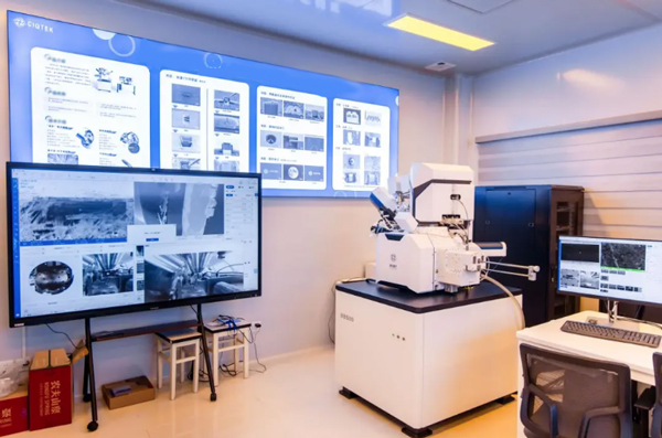
From September 23 to 25, 2025, CIQTEK made a strong impression at ARABLAB 2025, held at the Dubai World Trade Center. At Booth H1-C24 in Sheikh Saeed Hall 1, we demonstrated our latest scientific instruments and oilfield technologies to a diverse international audience.

CIQTEK Showcases Next-Generation Instruments at ARABLAB 2025


Highlights & Achievements

  • Comprehensive Portfolio Displayed
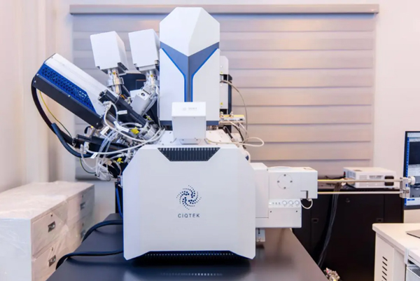
    We presented flagship systems in electron microscopy (FIB/SEM, TEM), nuclear magnetic resonance (NMR) spectrometers, and BET surface area & porosimetry analyzers—underscoring our commitment to advancing analytical science.

  • Integration of Oilfield Solutions under the QOILTECH Brand
    Under our specialized QOILTECH line, we introduced tools for petroleum exploration, including RSS, MWD/LWD systems, and near-bit gamma tools. These offerings were well received by participants seeking robust instrumentation for extreme environments.

  • Strong Engagement & Feedback
    At the booth, we addressed technical queries and shared success stories from across the research and industry sectors. Many attendees expressed interest in follow-up collaborations, demos, and trial opportunities.

  • Global Networking & Partnerships
    ARABLAB 2025 brought together distributors, end-users, and scientific institutions from across the world. CIQTEK strengthened relationships and opened dialogues for future regional projects and partnerships in the Middle East and beyond


CIQTEK thanks all visitors, partners, and colleagues who joined us in Dubai!

We look forward to continued collaboration and impactful research ahead!

Four-dimensional scanning transmission electron microscopy (4D-STEM) is one of the most cutting-edge directions in electron microscopy. By performing a two-dimensional scan across the sample surface while recording a full diffraction pattern at each scan point with a pixelated detector, 4D-STEM generates a four-dimensional dataset containing both real-space and reciprocal-space information.

This technique breaks through the limitations of conventional electron microscopy that typically collects only a single scattering signal. Instead, it captures and analyzes the entire spectrum of electron–sample interactions. With 4D-STEM, researchers can achieve multiple advanced functionalities within a single experiment, including virtual imaging, crystal orientation and strain mapping, electric and magnetic field distribution analysis (differential phase contrast), and even atomic-resolution reconstruction through diffraction stacking. It greatly expands the dimensionality and depth of materials characterization, offering an unprecedented tool for nanoscience and materials research.


At the Chinese National Conference on Electron Microscopy 2025 (Sept 26–30, Wuhan), CIQTEK releases its 4D-STEM solution, designed to break through the boundaries of traditional imaging and deliver data with unmatched dimensionality and analytical power.


System Workflow

CIQTEK Unveils 4D-STEM Solution for Advanced Electron Microscopy-workflow


The CIQTEK 4D-STEM solution features high spatial resolution, multi-dimensional analysis, low-dose operation to minimize beam damage, and flexible data processing, providing researchers with reliable and outstanding methods for advanced materials analysis.

Research on the microscopic behavior of materials is entering a new era of multi-scenario coupling and in-situ dynamic characterizationCIQTEK has launched an innovative In-situ Mechanical Testing Solution, designed with outstanding openness and compatibility. It enables seamless integration of CIQTEK’s full range of electron microscopes with mainstream in-situ testing devices, providing a flexible and efficient platform for coupled analysis in diverse research scenarios.


Breaking the limitations of closed systems, the solution integrates all critical elements required for in-situ EM adaptability, featuring:

  • High beam current: >100 nA, ideal for fast EDS/EBSD analysis

  • Large space: 360 × 310 × 288 mm (L × W × H)

  • High load capacity: 5 kg (up to 10 kg with custom fixtures)

  • Multi-view CCDs: ensuring system safety during in-situ operation

  • Multiple interfaces: supporting customized flange accessories

  • Pre-acceptance: full accessory debugging before delivery, ensuring complete functionality without on-site installation issues

The solution can be configured across CIQTEK’s full range of electron microscopy products, including CIQTEK SEM3200SEM5000XDB550 dual-beam systems, and more. It also offers seamless compatibility with tensile stages, heating stages, nanoindenters, and electrochemical workstations from world-leading suppliers. This open architecture enables researchers to flexibly combine the most suitable equipment, maximizing experimental performance.


CIQTEK’s in-situ stage solution supported customers in publishing a high-impact paper (DOI: 10.1126/science.adq6807).

CIQTEK In-situ Mechanical Testing Solution for SEM


CIQTEK’s In-situ Mechanical Solution also supports multi-field coupling (mechanical, thermal, electrochemical), enabling nanoscale real-time observation of materials under complex environments. By synchronizing high-resolution imaging with in-situ signals, researchers can capture critical phenomena such as crack propagation, phase transitions, and interfacial reactions with precision.

With a temperature range of -170 to 1200 °C, advanced load control, and rapid response systems, it accurately simulates service conditions of materials across various industries. Combined with EBSD and EDS, it provides comprehensive datasets for understanding material behavior under coupled stimuli.


Successfully applied in aerospace materials, new energy devices, and biomedical materials, this solution demonstrates CIQTEK’s exceptional compatibility and scalability in advanced electron microscopy platforms.

In life sciences, achieving high-precision and large-scale 3D structural and dynamic analysis of biological samples such as cells and tissues has become key to breaking through research bottlenecks. CIQTEK has introduced a multi-technology-route Volumetric Electron Microscopy (VEM) solution, integrating SS-SEM, SBF-SEM, and FIB-SEM. This provides an all-around, high-performance, and intelligent platform for biological 3D reconstruction, helping researchers uncover the micro-level mysteries of life.


Three Advanced Technical Routes

01. SS-SEM High-Speed Imaging
By combining external serial sectioning with the CIQTEK high-speed HEM6000-Bio SEM, this solution enables rapid imaging and automated acquisition of large-volume samples. Data acquisition efficiency is more than 5× higher than conventional SEM, supporting 24/7 unattended high-throughput operation.


02. SBF-SEM In-Situ Sectioning
Based on the CIQTEK ultra-high-resolution SEM5000X with an integrated microtome, this approach achieves in-situ sectioning and imaging cycles. It offers simple operation, high automation, and effectively avoids surface contamination.


03. FIB-SEM High-Precision Analysis
Leveraging focused ion beam–electron beam dual-beam systems, this route delivers nanoscale Z-axis resolution to analyze fine structures such as organelles and membranes. It enables in-situ 3D reconstruction without physical slicing.


Intelligent Integration & Broad Applications

The CIQTEK VEM solution deeply integrates AI algorithms and a multilingual software platform, supporting a full workflow from data acquisition, image alignment, and segmentation to 3D visualization. Compatible with mainstream reconstruction software, it significantly lowers the learning curve.


Application cases span neuroscience, cell biology, and pathogenic microbiology, offering a powerful tool for advancing life science research.

CIQTEK Volumetric Electron Microscopy (VEM) Solution

As semiconductor manufacturing advances to finer process nodes, wafer-level defect analysis, failure location, and micro-nano fabrication have become key to improving yield. CIQTEK introduces the 8-inch Wafer Dual-Beam Full-Size Processing Solution, combining high-resolution imaging and precise ion beam processing to achieve "observation-analysis-cutting" across the entire wafer, providing strong technical support for advanced semiconductor processes.


This solution features a 150mm long-stroke high-precision sample stage, enabling full-wafer, non-destructive observation and processing of 8-inch wafers. With an external optical navigation system and intelligent anti-collision algorithms, it ensures rapid and precise wafer positioning and safe operation. The system is equipped with a Schottky field emission electron gun, offering a resolution of 0.9 nm @ 15kV, and an ion beam resolution of 3 nm @ 30kV, capable of defect detection, cross-section slicing, and micro-structure fabrication at the nanoscale.


Core Advantages:

  • 150mm Travel Stage:
    • Combines long travel with high precision for an extensive observation range.

    • Excellent compatibility with different-sized fixtures.

    • Robust structure ensures wafer stability and quick, reliable loading.

  • 8-inch Quick Exchange:
    • Intelligent weight-bearing design with a sliding base for stability and durability.

    • Full-size compatibility: Supports 2/4/6/8-inch wafers.

    • Fast sample exchange: Vacuum pumping and sample loading within one minute.

  • Software and Anti-Collision:
    • Fully automatic intelligent navigation with accurate movement and positioning.

    • Multi-axis coordinated motion for full-wafer observation.

    • Smart anti-collision: Trajectory simulation and algorithmic spatial calculations to avoid risks.

    • Multiple real-time monitoring: Real-time multi-angle monitoring of wafer position.

  • External Optical Navigation:

    • Ultra-stable structure design suppresses image shake.

    • High-definition imaging with a precise field of view for full-wafer display.

    • Professional anti-glare lighting reduces wafer surface reflection.


Wafer observation range

Wafer observation range


CIQTEK Dual-Beam Electron Microscope Solution combines outstanding hardware with intelligent software systems, enabling efficient defect detection and process optimization through one-click brightness and contrast adjustment, auto-focus, and multi-format image output, empowering users to complete the full chain of tasks from defect discovery to process optimization.

In today’s fast-paced world, keeping track of your health and fitness has never been more important. The ET585 smartwatch brings cutting-edge technology directly to your wrist, offering a comprehensive suite of features designed to monitor, manage, and improve your well-being.


The 2.04-inch AMOLED Retina full-touch display delivers vibrant visuals with a 368×448 resolution, making it easy to navigate through apps, health metrics, and notifications. Built for professional health monitoring, ET585 includes ECG and HRV detection, 30-second micro physical examinations, and full-day heart rate monitoring to help detect early signs of arrhythmia and assess cardiovascular health. Blood oxygen, blood pressure, and even non-invasive blood sugar monitoring keep track of essential physiological parameters, while body composition and BMI measurement provide deeper insight into your fitness progress. Emotional fatigue detection and women’s health tracking further personalize your wellness experience.


Fitness enthusiasts will love ET585’s support for over 130 sports modes, step counting, calorie tracking, and distance measurement. The watch also monitors sleep patterns scientifically, analyzing snoring and respiratory risks for better rest.


Beyond health and fitness, ET585 integrates smart lifestyle features such as Bluetooth calling, music playback and control, NFC access, alarms, weather updates, flashlight, games, and a voice assistant.


Whether you’re tracking your daily steps, monitoring heart health, or staying connected on the go, ET585 combines precision, style, and intelligent functionality into one sleek wearable. It’s more than a smartwatch—it’s a personal health companion that adapts to your lifestyle and empowers you to live smarter and healthier.

NFC access control smart wearable


Palm Vein Scanner swiping technology, a cutting-edge biometric technology, provides comprehensive support for identity verification. Based on a proprietary multimodal palm swiping camera and paired with SFT biometric algorithms, palm swiping technology significantly improves the security and efficiency of identity verification, enabling rapid authentication and permission management in all scenarios. Furthermore, the contactless service provided by this technology effectively reduces the risk of contact transmission, improves public health and safety, and provides a superior user experience.


Palm Prints scanner in Transportation:

 Airport Line

China's first subway line to feature palm-swipe payment ushers in a new era of "contactless travel."

The implementation of the palm-swipe system on the Daxing Airport Line marks the official entry of rail transit into the biometric 3.0 era. Palm-swipe biometric technology redefines subway travel and ushers in a new era of "contactless travel" in smart transportation. This not only significantly improves passenger travel efficiency but also promotes the deep integration of artificial intelligence technology in public services.


Palm prints scanner in transporation


Wireless Palm vein swiping module used  in Stadium:


Palm vein scanner in sports

Swimming Pool

"One-Palm Access": China's first large-scale sports venue full-scene palm scanning application demonstration project

The  Swimming Pool of the National Olympic Center has officially launched its "Palm Scan Access" system. Leveraging innovative multimodal biometric technology, this system redefines the sports and fitness experience, offering contactless access throughout the entire experience with just one palm, creating a new model for smart sports venue services.


Gym

Palm Check-in: A New Smart Fitness Experience

Gym's palm check-in marks the first application of palm-scanning biometrics in the fitness industry. Leveraging multimodal biometric technology, it enables contactless, ultra-fast identity verification, effectively addressing issues such as card fraud, long queues, and unsanitary conditions associated with traditional QR code check-in.


Palm vein Payment Reader in Retailing:


WeChat Payment Palm vein scanner


 7-Eleven Convenience Stores

Over 1,500 stores now support palm payment, offering a new "swipe and pay" experience.

As one of the first convenience store brands nationwide to support WeChat palm payment, over 1,500 7-Eleven stores now support palm payment. This feature uses palm biometric recognition technology for contactless checkout, improving overall efficiency, further reducing queues, and accelerating the intelligent upgrade of retail services.


Contactless Palm vein scanner in Schools:

University

China's first university "Campus One-Person Pass" system

Shenzhen University's "Campus One-Person Pass" system uses palm-swipe biometric technology to provide a secure, contactless authentication experience. After users first enter their palm print on a palm-swipe device and link it to their WeChat campus code, they can pay instantly in cafeterias, convenience stores, and other locations, without the need for a phone or physical card.


Biometric Palm Vein scanner in Shared charging

Biometric Palm vein reader

Jiedian

1-second identification, 2-step operation, 5-second delivery


Jiedian's palm-swipe charging service revolutionizes shared charging services with biometric recognition technology. Leveraging cutting-edge multimodal biometrics, it quickly and accurately completes the identification process, further addressing traditional shared charging pain points such as dead phones or poor signal quality, delivering a superior shared charging experience.