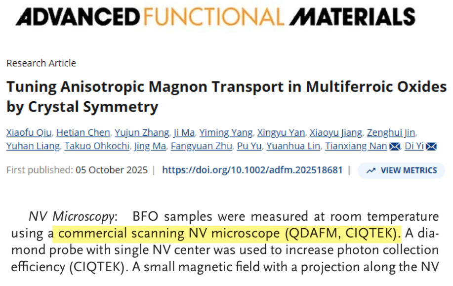
In the fields of high-temperature material performance research and phase transition mechanism analysis, traditional external heating methods often fail to combine precise micro-region temperature control with real-time observation.


CIQTEK, in collaboration with the Micro-Nano Center of the University of Science and Technology of China, has developed an innovative in-situ heating chip solution. By integrating MEMS heating chips with dual-beam electron microscopes, this solution enables precise temperature control (from room temperature to 1100°C) and micro-dynamic analysis of samples, offering a new tool for studying material behavior in high-temperature environments.

This solution uses the CIQTEK dual-beam SEM and specialized MEMS heating chips, with temperature control accuracy better than 0.1°C and temperature resolution better than 0.1°C. The system also features excellent temperature uniformity and low infrared radiation, ensuring stable analysis at high temperatures. The system supports various characterization techniques during heating, including micro-region morphology observation, EBSD crystal orientation analysis, and EDS composition analysis. This allows for a comprehensive understanding of phase transitions, stress evolution, and composition migration under thermal effects.


The system operates without breaking the vacuum, fulfilling the full process requirements for sample preparation and characterization (in-situ micro-region EBSD).

CIQTEK Launches In-situ Heating Chip Solution for High-Precision Analysis

CIQTEK Launches In-situ Heating Chip Solution for High-Precision Analysis


The integrated workflow design covers the entire process, from sample preparation (ion beam processing, nano-manipulator extraction) to in-situ welding and heating tests. The system supports multi-angle operation, featuring a 45° heating chip and a 36° copper grid position, which meet the complex experimental needs. The system has been successfully applied in high-temperature performance research of alloys, ceramics, and semiconductors, helping users gain deeper insights into material responses in real-world environments.


September 26–30, Wuhan | 2025 Chinese National Conference on Electron Microscopy
CIQTEK's eight major electron microscopy solutions will be showcased!

In data centers, DAC (Direct Attach Copper) and AOC (Active Optical Cable) are two commonly used high-speed connectivity cables. They may look similar in appearance but differ significantly in functionality and application scenarios. Understanding the differences between them helps make more appropriate choices when building or upgrading data centers.

QSFP28 to QSFP28 AOC cable

What is a DAC Cable?


A DAC cable is a copper-based cable with standard connectors (such as SFP+, QSFP+) at both ends. It transmits electrical signals directly without the need for additional signal conversion modules.
Its characteristics are obvious: the transmission distance is short - passive DACs typically reach only 3-7 meters, and active DACs max out at 15 meters. However, it has low cost and low power consumption - passive ones consume almost no power, and active ones operate within 1W. Nevertheless, the copper material makes it susceptible to electromagnetic interference, making it more suitable for short-distance scenarios with simple electromagnetic environments.
In data centers, DACs are commonly used for device connections within the same rack (e.g., between servers and switches) or short-distance interconnections between adjacent racks (within 10 meters). They enable high-speed transmission from 10Gbps to 100Gbps at a relatively low cost.
 
What is an AOC Cable?
 
An AOC cable features multi-mode optical fiber as its core, with integrated optical transceivers at both ends. During operation, electrical signals are first converted to optical signals for transmission through the fiber, then converted back to electrical signals at the destination.
Its advantage lies in long-distance transmission: using OM3 fiber can reach 100 meters, and some products even exceed 300 meters. Additionally, optical fiber is immune to electromagnetic interference, ensuring strong signal stability. However, it has higher costs and power consumption (around 1-2W) due to the need for optical transceivers for signal conversion.
AOCs are suitable for long-distance connections in data centers, such as interconnections between cross-rack or cross-floor devices, or scenarios with extremely high requirements for signal quality like high-performance computing and financial transactions. They support high-speed transmission from 10Gbps to 400Gbps.
 
 
Core Differences and Selection Recommendations
 
The core differences can be summarized as: DAC uses copper to transmit electrical signals, offering short distance, low cost, and susceptibility to interference; AOC uses optical fiber to transmit optical signals, providing long distance, anti-interference capability, and higher cost.
When making a selection, first consider the distance: prioritize DAC for distances within 10 meters, as it is cost-effective and sufficient; choose AOC for distances exceeding 10 meters to ensure stable transmission. Additionally, AOC is more reliable in complex electromagnetic environments or scenarios requiring long-term high bandwidth; DAC is more economical for short-distance connections with limited budgets.
In conclusion, DAC and AOC each have their strengths. Data centers usually use them in combination according to specific connection requirements to ensure efficiency while controlling costs.
 
Boasting over 100 product testing devices, every DAC and AOC cable from Fiberwdm meets stringent standards. Their dedicated technical support team addresses all product - related issues, from operation to technical challenges. Whether you need a cost - effective short - range DAC or a high - performance long - distance AOC, Fiberwdm delivers tailored solutions to enhance your data center's stability and efficiency.​


Passive Optical Network (PON) is the core technology for fiber-optic broadband. Leveraging the advantages of "passivity" (no power supply required for the Optical Distribution Network/ODN), low cost, high reliability, and wide coverage (up to 20 km), it has become the mainstream of broadband networks. GPON, XG-PON, and XGS-PON represent three key phases in the evolution of PON technology, with core differences centered on bandwidth capability and symmetry—factors that directly define their technical positioning. This article examines the core distinctions among the three from the perspectives of technological evolution, core parameters.


I. Technological Evolution: The Iteration Logic from "Basic Gigabit" to "Symmetric 10G"

 
The evolution of these three technologies is essentially a process of "bandwidth expansion" and "symmetry optimization". All comply with standards set by the ITU-T (International Telecommunication Union-Telecommunication Standardization Sector), with gradually improved compatibility:


  • GPON: Launched in the 2000s as the "first-generation gigabit PON," it addressed the transition from "100-Mbps broadband" to "gigabit access" and served as the primary technology for early Fiber-to-the-Home (FTTH) deployments.
  • XG-PON: Introduced in the 2010s as the "second-generation PON," it targeted download-intensive needs (e.g., high-definition videos, cloud gaming) by increasing downstream bandwidth to 10G, driving the popularization of "gigabit home access."
  • XGS-PON: Commercialized in the 2018s as the "third-generation PON," it addressed XG-PON’s upstream bandwidth limitations by enabling "symmetric 10G upstream/downstream," making it suitable for scenarios requiring high bidirectional bandwidth.


GPON XGS-PON NG-PON


II. Comparison of Core Parameters: A Clear Overview of Differences


Comparison Dimension

GPON (Gigabit PON)

XG-PON (10G PON) XGS-PON (Symmetric 10G PON)
Standards Basis ITU-T G.984 Series ITU-T G.987 Series ITU-T G.9807 Series

Upstream/Downstream Bandwidth

Symmetric 1.25 Gbps Asymmetric (10 Gbps downstream, 2.5 Gbps upstream) Symmetric 10 Gbps (upstream/downstream)
Typical User Speed Mostly 100-Mbps class (50-100 Mbps), with some gigabit speeds 1-Gbps class downstream (500 Mbps-1 Gbps), 100-Mbps class upstream Symmetric 1-Gbps class (500 Mbps-1 Gbps)
Bandwidth Symmetry Symmetric Asymmetric Symmetric
Maximum Splitting Ratio 1:64 (supports 64 user splits) 1:128 1:128
Core Technical Features Mature and stable, low cost; supports triple-play (voice, data, video) Significantly enhanced downstream bandwidth; suitable for download-intensive scenarios Balanced upstream/downstream bandwidth; supports high bidirectional bandwidth scenarios


III. Demand-Driven Technological Iteration

 
From GPON to XG-PON and then to XGS-PON, this evolution is not a case of "new technologies completely replacing old ones," but rather a typical example of "demand-driven advancement":
 
  • GPON has laid the foundation for Fiber-to-the-Home (FTTH). With its mature technology and low cost, it addresses the "from scratch" need for broadband access, and still serves scenarios with low bandwidth requirements today.
  • XG-PON has broken through downstream bandwidth bottlenecks. Its asymmetric design matches users' "download-prioritized" needs, making it the mainstream technology for current home gigabit broadband.
  • XGS-PON achieves balanced bidirectional bandwidth. Equipped with symmetric 10G capability, it adapts to new scenarios such as 5G and cloud storage, and represents the core evolutionary direction of optical networks in the next 5-10 years.


The core logic of these three technologies has always been "matching current and short-term bandwidth needs at a reasonable cost," and together they form a complete technical system for optical networks, covering everything from basic services to future upgrades.


Explore Fiberwdm's GPON, XG-PON and XGS-PON products.


When you upload work files via gigabit broadband while smoothly streaming 4K IPTV programs, you may not realize that behind these "simultaneous online" high-speed experiences lies an "intelligent dispatcher of optical signals" — the PON Coexistence Wavelength Division Multiplexer (CEx-WDM). It not only makes "one optical fiber for all services" a reality but also serves as the core driver for future 10G and beyond-10G broadband upgrades.
 
PON XGS-PON CATV Device


1. "Classify and Package" Optical Signals to Turn One Fiber into a "Multi-Lane Highway"

In optical fiber communication, optical signals for different services (such as internet access, TV viewing, and network testing) originally required separate fibers. The core of the CEx-WDM device is using Wavelength Division Multiplexing (WDM) to "attach wavelength labels" to optical signals: it classifies and packages data streams from GPON (gigabit broadband), XGS-PON (10G broadband), NG-PON2 (next-generation ultra-high-speed broadband), even RF signals for Cable Television (CATV) and maintenance signals for Optical Time-Domain Reflectometry (OTDR) by "wavelengths", enabling them to transmit simultaneously in a single fiber without interference.


To illustrate, it’s like assigning "dedicated lanes" (different wavelengths) to traffic bound for different destinations, creating a "multi-lane highway" within one optical fiber. This eliminates the need for duplicate fiber laying while allowing all services to "run at full speed".
 

2. Old Broadband Upgrades to New Broadband in Seconds Without Changing Fibers

For many households and enterprises, existing networks still operate at the GPON (gigabit-level) or even EPON (100 Mbps-level) stage. With CEx-WDM, operators can upgrade old networks "in one step" to XGS-PON (10G symmetric broadband) without laying new fibers, and smoothly transition to NG-PON2 (supporting over 40G ultra-high speed) in the future.


Imagine this: The optical fiber installed in your community years ago could only support gigabit speeds, but after adding this device, you can directly access 10G broadband without digging walls or rewiring. Transferring large files or hosting 8K video conferences becomes seamless — this is the magic of "upgrading without changing fibers".
 

3. From Households to Future Technologies, It Exists Everywhere

The application scenarios of this device have long permeated all aspects of our lives and industries:


  • Households & Communities: In a community’s optical distribution box, it distributes "multi-service signals" from the main fiber to each household, enabling simultaneous use of "gigabit broadband + IPTV + cable TV" with a seamless experience.
  • Operator Machine Rooms: On the side of OLT (Optical Line Terminal) devices in core machine rooms, it acts as a "central signal dispatching room", efficiently integrating GPON/XGS-PON signals from thousands of households with CATV and OTDR signals before connecting to the urban backbone network.


Future Scenarios: It also paves the way for "future demands" like 5G base station backhaul, industrial internet (e.g., low-latency networking for hundreds of devices in smart factories), and metaverse interaction — NG-PON2 technology allows a single fiber to carry over 40G bandwidth, sufficient to support technological evolution for a decade or more.


4. It is the "Invisible Driver" of Broadband Upgrades, Changing More Than Just Speed

For operators, CEx-WDM means cost savings and convenience: they can launch multiple services (gigabit broadband, 10G dedicated lines, high-definition TV, etc.) simultaneously without repeating fiber network construction. For users, it brings a leap in experience — from "merely accessing the internet" to "high-speed internet + simultaneous multi-services". In the future, watching 8K videos or playing metaverse games will no longer suffer from stutters due to "insufficient bandwidth".


In short, this tiny passive device is a crucial step for optical fiber broadband to move from "popularization" to "ultimate experience", silently propelling our digital lives toward higher speeds and richer possibilities.

In the wave of digitalization, high-speed data transmission and processing have become the core driving forces behind technological development. As a key carrier of information transmission, optical communication technology continues to evolve to meet the explosive growth in bandwidth demand. Among these advancements, the LPO optical module has emerged with unique technological advantages, standing out as a breakthrough technology in the field of optical communication.
 

I. Definition of LPO Optical Module

 
LPO stands for Linear-drive Pluggable Optics. Its core features lie in the combination of linear drive technology and pluggable characteristics.


  • Pluggable characteristics: Similar to USB devices, it supports flexible plug-and-play, greatly improving the convenience of equipment installation, maintenance, and upgrades, while significantly reducing operational costs and downtime in scenarios such as data centers.
  • Linear drive technology: This is the core difference between LPO and traditional optical modules. Traditional optical modules rely on DSP (Digital Signal Processing) chips for signal processing, which suffer from high power consumption and high costs. In contrast, LPO optical modules abandon DSP chips and adopt linear analog technology to directly drive optoelectronic devices, simplifying the signal processing and optimizing energy efficiency.


II. Working Principle of LPO Optical Module

 
The core function of an LPO optical module is to realize efficient conversion between electrical and optical signals, with its working process centered on "simplified processing":


  • Transmitting end: After receiving an electrical signal, it is processed by a high-linearity Driver chip with CTLE (Continuous Time Linear Equalization) function to compensate for high-frequency attenuation during transmission. Then, the laser is directly driven to convert the electrical signal into an optical signal, which is sent through an optical fiber.
  • Receiving end: The optical detector converts the received optical signal into a weak electrical signal, which is amplified and equalized by a TIA (Transimpedance Amplifier) with EQ (Equalization) function. After restoring the signal integrity, it is transmitted to the terminal equipment.


The entire process replaces the traditionally complex DSP processing with simple signal compensation, significantly reducing power consumption and costs while ensuring transmission quality.
 
LPO Optical Module


III. Technical Advantages of LPO Optical Module

 
Compared with traditional optical modules, the advantages of LPO are concentrated in three dimensions: "low consumption, low cost, and high efficiency":


  • Low power consumption: After removing the DSP chip, the power consumption of a 400G LPO module can be reduced to below 4W, which is about 50% lower than traditional solutions, directly reducing electricity bills and cooling costs in data centers.
  • Low cost: Eliminating the high-cost DSP chip reduces material costs by 15-20%. At the same time, the simplified structure also lowers manufacturing costs, laying the foundation for large-scale applications.
  • Low latency: By skipping the DSP processing link, the delay is reduced from the nanosecond level to the sub-nanosecond level, a reduction of more than 30%, perfectly meeting the strict real-time requirements of AI training, high-frequency trading, and other scenarios.
  • Compatibility and flexibility: It retains the traditional pluggable package, enabling seamless compatibility with existing network hardware. Moreover, it supports data rates from 100G to 800G and even higher, adapting to diverse scenario needs.


IV. Application Scenarios of LPO Optical Module

 
With its unique technical advantages, LPO optical modules show strong competitiveness in the following scenarios:


  • Data center internal interconnection: In short-distance scenarios of 100 meters to 2 kilometers, its low power consumption and low cost can efficiently meet the connection needs between servers and switches, improving the overall operational efficiency of data centers.
  • AI computing power clusters: The low-latency feature precisely matches the intensive communication patterns in AI training, ensuring fast data transmission in 10,000-card-level clusters, avoiding network bottlenecks, and enhancing the overall computing power performance of the cluster.


V. Challenges and Countermeasures of LPO Optical Module

 
Despite its significant advantages, LPO optical modules still need to overcome the following bottlenecks:


  • Transmission distance limitation: Due to the lack of DSP processing, the communication distance is limited, and it is currently mainly applicable to medium and short distances. Countermeasures include: adopting silicon photonics integration technology and advanced packaging processes to improve signal stability, and introducing intelligent compensation algorithms to optimize transmission performance.
  • High precision requirements for craftsmanship: Strict requirements for the matching accuracy of optical devices and circuit parameters necessitate enterprises to improve precision manufacturing capabilities and strengthen cooperation across the industrial chain to unify standards.
  • Standardization issues: The lack of unified industry standards affects the compatibility and interoperability of products from different manufacturers. Currently, industry associations and standardization organizations are accelerating the formulation of relevant technical specifications to promote industrialization.


VI. Future Development Trends of LPO Optical Module

 
With technological iteration, the development direction of LPO optical modules is gradually becoming clear:


  • Continuous technological innovation: Developing higher-performance optical devices, optimizing circuit design and compensation algorithms, and integrating emerging technologies such as AI to realize intelligent management and adaptive adjustment of modules.
  • Expansion of application fields: Extending from data centers and AI clusters to 5G communication, high-performance computing, intelligent transportation, and other fields, helping various industries achieve digital transformation.
  • Multi-technical collaboration: Forming complementary advantages with technologies such as CPO (Co-packaged Optics) and coherent optical communication to build full-scenario optical communication solutions covering short, medium, and long distances, meeting diversified transmission needs.


By simplifying technology to balance performance and cost, LPO optical modules are reshaping the technical landscape of the optical communication field. With the gradual resolution of existing challenges, they are expected to become the core solution for high-speed short-distance communication in the future, providing key support for the development of the digital economy.
 

How Can AD255C High Frequency PCBs Enhance Your RF and Microwave Designs?


In the rapidly evolving world of telecommunications and high-speed electronics, the demand for advanced printed circuit boards (PCBs) that can perform reliably at high frequencies is greater than ever. Among the leading materials engineered to meet these challenging requirements is the Rogers AD255C laminate—a premier choice for high-frequency PCB applications. This article explores the key attributes, manufacturing capabilities, and practical applications of AD255C High Frequency PCBs, illustrating why they are an optimal solution for cutting-edge RF and microwave systems.

An Introduction to AD255C High Frequency Laminates

Rogers AD255C laminates represent a sophisticated class of high-performance materials, formulated through a precise combination of fluoropolymer resin, specialized ceramic fillers, and reinforced fiberglass. This unique composition capitalizes on the outstanding thermal and electrical characteristics of fluoropolymer, augmented by the mechanical stability offered by ceramic and glass reinforcement. The result is a high-frequency substrate that delivers remarkably low signal loss, reduced passive intermodulation (PIM), and excellent control over thermal expansion. These properties make AD255C an ideal candidate for a wide range of telecommunication and RF applications where signal integrity and thermal management are critical.


Salient Features of AD255C High Frequency PCBs


 Features of AD255C High Frequency PCBs


1) Ultra-Low Loss Composite Structure:

The AD255C material is based on a polytetrafluoroethylene (PTFE) matrix enriched with ceramic micro-fillers. This composite ensures minimal dielectric loss, making it exceptionally suitable for high-speed and high-frequency circuit designs where signal attenuation must be kept to an absolute minimum.

2) Exceptional Loss Tangent Performance:

With an impressively low dissipation factor of 0.0014 measured at 10 GHz—typical for base station operating frequencies—this laminate facilitates highly efficient RF signal transmission. This leads to improved energy efficiency, reduced heat generation, and enhanced overall system performance.


3) Stable Dielectric Constant:

The AD255C material offers a consistent dielectric constant (Dk) of 2.55, which is maintained within tight tolerances. This uniformity ensures predictable impedance matching and reliable signal propagation, which are essential in sensitive high-frequency and microwave applications.


4) Low-Profile Copper Foil:

The inclusion of electro-deposited low-profile copper enhances electrical conductivity while supporting finer line patterning and improved etching resolution. This feature is especially beneficial in compact and densely populated PCB layouts.


5) Controlled Thermal Expansion:

The coefficient of thermal expansion (CTE) in the Z-direction is limited to 50 ppm/°C. This low CTE value significantly improves dimensional stability across varying temperatures, reducing the risk of plated-through-hole failure and ensuring long-term reliability under thermal cycling.


PCB Manufacturing Capabilities with AD255C Materials


PCB Manufacturing Capabilities with AD255C Materials


We support the fabrication ofhigh-frequency PCBs using AD255C substrate with the following capabilities:


Board Construction: Options include double-layer, multilayer, and hybrid PCB structures, supporting both standard and high-complexity designs.


Copper Weight and Dielectric Thickness: Available copper weights include 1 oz (35 µm) and 2 oz (70 µm). Dielectric thickness can be selected from 20 mil (0.508 mm) up to 125 mil (3.175 mm).


Panel Size: Maximum panel dimensions of 400 mm x 500 mm are supported, accommodating either one large board or multiple arrays.


Solder Mask Variants: Multiple color options are available including Green, Black, Blue, Yellow, Red, Purple, and more.


Surface Finishes: We offer a comprehensive selection of surface treatments such as Immersion Gold (ENIG), HASL, Immersion Silver, Immersion Tin, OSP, ENEPIG, Bare Copper, and Full Gold Plating.


AD255C PCBs


Typical Applications

AD255C PCBs are widely used in applications where signal integrity and thermal performance are paramount. Common use cases include:


  • Cellular infrastructure equipment including 5G base station antennas
  • Automotive telematics and radar antenna systems
  • Satellite communication equipment and commercial radio antennas
  • Aerospace and defense communication systems
  • High-speed data transmission and microwave radio links


Conclusion

The Rogers AD255C High Frequency PCB material offers a compelling blend of low loss, stable electrical properties, and excellent thermal characteristics, making it an outstanding substrate for advanced RF and microwave applications. With extensive manufacturing flexibility and a wide range of finishing options, we are well-equipped to support your high-frequency PCB requirements with reliability and precision.

How Can TLY-5Z High Frequency PCBs Enhance Thermal and Dimensional Stability in Your Designs?


In the world of high-frequency electronics, the choice of printed circuit board (PCB) material is critical to achieving optimal performance, especially in demanding sectors such as aerospace and communications.TLY-5Z high frequency PCBs stand out as an advanced solution, specifically engineered to deliver exceptional electrical and mechanical properties under challenging conditions.


Taconic TLY-5Z laminates are composite materials that combine glass-filled polytetrafluoroethylene (PTFE) with woven fiberglass reinforcement. This unique construction is tailored for applications where low density is essential—such as in aerospace systems—where every gram matters. Unlike unreinforced PTFE materials, Taconic TLY-5Z PCB offers outstanding dimensional stability, significantly reducing Z-axis expansion. This property is uncommon in conventional PTFE-rich composites and is crucial for maintaining structural integrity under thermal stress.


A key advantage of TLY-5Z Taconic RF PCB Circuit Board is its superior thermal management. When compared to standard low-Dk PTFE composites, it demonstrates enhanced resistance against z-axis expansion, which in turn minimizes stress on plated through-holes. This ensures greater reliability during thermal cycling and improves drilling precision during the manufacturing process.


Key Properties of TLY-5Z Laminates


Key Properties of TLY-5Z Laminates

Adhering to IPC standards, TLY-5Z exhibits a range of impressive material characteristics:


  • Specific Gravity: 1.92 g/cm³(IPC-650 2.3.5)
  • Dielectric Constant (Dk): 2.20±0.04 at 10 GHz (IPC-650 2.5.5.5.1)
  • Dissipation Factor (Df): 0.0015 at 10 GHz (IPC-650 2.5.5.5.1)
  • Coefficient of Thermal Expansion (CTE):
  • X-axis: 30 ppm/°C
  • Y-axis: 40 ppm/°C
  • (measured between 25°C and 260°C per IPC-650 2.4.41)


These properties make TLY-5Z twice as dimensionally stable as traditional PTFE substrates. Such thermal stability allows for improved drilling quality and supports repeated thermal cycles without failure. Moreover, the material facilitates easy grounding and stitching along high-frequency transmission lines, which is essential for signal integrity in RF designs.


Additionally, TLY-5Z boasts minimal moisture absorption—only 0.03% as per IPC-650 2.6.2.1—and a UL-94 V-0 flammability rating, making it both highly reliable and safe for critical applications.


PCB Manufacturing Capabilities with TLY-5Z


PCB Manufacturing Capabilities with TLY-5Z


We support a wide range of PCB configurations to meet diverse design requirements:


  • Board Types: Single-sided, Double-sided, Multilayer, and Hybrid constructions
  • Copper Weights: 1oz (35µm) or 2oz (70µm)
  • Laminate Thickness: 10mil (0.254mm), 20mil (0.508mm), 30mil (0.762mm), and 60mil (1.524mm)
  • Maximum PCB Dimensions: 400mm x 500mm
  • Solder Mask Colors: Green, Black, Blue, Yellow, Red, and others
  • Surface Finishes: Bare Copper, HASL, ENIG, Immersion Silver, Immersion Tin, ENEPIG, OSP, and Pure Gold Plating


These options provide designers with the flexibility to optimize their high-frequency circuits for performance, durability, and aesthetic requirements.


TLY-5Z Taconic PCBs


Typical Applications

TLY-5Z Taconic PCBs are widely used in applications where lightweight, stable, and reliable performance is non-negotiable. Common uses include:


  • Aerospace communication and navigation systems
  • Lightweight antennas for aircraft and satellites
  • RF passive components including filters, couplers, and power dividers
  • Advanced radar and wireless infrastructure


Whether for prototyping or high-volume production,TLY-5Z Taconic RF PCB provide a future-proof solution for next-generation high-frequency electronic devices.


Is RO4725JXR the Optimal Cost-Effective Solution for Your High-Frequency PCB Design Needs?


In the rapidly evolving world of wireless communication, the demand for high-performance, reliable, and cost-effective printed circuit boards (PCBs) is greater than ever. For engineers and designers working on cutting-edge RF and antenna systems, the choice of substrate material is critical. RO4725JXR high-frequency PCB emerge as a premier solution, expertly engineered to meet the stringent requirements of modern high-frequency applications while offering exceptional value and manufacturability.


Introduction to RO4725JXR High-Frequency Laminates


RO4725JXR is an antenna-grade laminate constructed from a sophisticated composite of hydrocarbon, ceramic, and woven glass. This unique formulation endows the dielectric material with a suite of properties that are indispensable for optimal antenna performance. A significant advantage of Rogers RO4725JXR is its full compatibility with standardFR-4 multilayer board processing and high-temperature lead-free assembly workflows. Unlike traditional polytetrafluoroethylene (PTFE) based materials, which often necessitate specialized and costly through-hole preparation treatments, RO4725JXR PCB simplifies the manufacturing process. This elimination of extra steps positions it as a highly cost-competitive alternative to conventional PTFE antenna materials, allowing design engineers to strike a perfect balance between superior radio frequency performance and overall project budget.


Outstanding Material Properties and Features


The superiority of RO4725JXR is defined by its exceptional electrical and thermal characteristics, each contributing to enhanced signal integrity and reliability in high-frequency environments.


RO4725JXR features


1) Controlled Dielectric Constant (Dk): RO4725JXR boasts a low and exceptionally stable dielectric constant of 2.55±0.05, measured at 10 GHz. This precision ensures consistent impedance control and minimizes signal propagation delays, which is vital for maintaining signal fidelity in high-speed RF circuits.


2) Low Z-Axis Coefficient of Thermal Expansion (CTE): With a Z-axis CTE of 25.6 ppm/°C, the material demonstrates remarkable dimensional stability across a wide temperature range. This property is crucial for preventing via failures, as it significantly reduces the risk of plated through-holes cracking during thermal cycling, thereby enhancing the long-term reliability of the PCB assembly.


3) Excellent Thermal Coefficient of Dk (TCDk): The thermal coefficient of the dielectric constant is a remarkably low +34 ppm/°C. This ensures that the electrical properties of the material remain stable and predictable even as operating temperatures fluctuate, preventing performance drift in critical applications.


4) Minimal Dissipation Factor (Df): At 10 GHz, the laminate exhibits an ultra-low dissipation factor of just 0.0026. This low loss tangent translates to minimal signal energy being lost as heat, thereby improving efficiency and enabling clearer signal transmission over longer distances with reduced attenuation.


5) High Glass Transition Temperature (Tg): Featuring a Tg exceeding 280°C, RO4725JXR retains its mechanical rigidity and electrical properties even when subjected to the high temperatures encountered during lead-free soldering and harsh operational conditions.


6) Reduced Passive Intermodulation (PIM): A standout feature for antenna applications is its superior Passive Intermodulation performance, with a typical PIM value of -166 dBC. This low PIM is essential for minimizing interference and maintaining signal clarity in high-power multi-carrier cellular antenna systems, directly boosting overall antenna performance.


Comprehensive PCB Manufacturing Capabilities


To fully leverage the advantages of RO4725JXR material, our manufacturing services offer extensive capabilities tailored to your specific project requirements.


RO4725JXR PCB Manufacturing Capabilities


We provide a complete range of PCB constructions, from simple single-sided and double-sided boards to complex multi-layer and hybrid designs. This versatility makes our services ideal for everything from basic electronic devices to sophisticated communication infrastructure.


To achieve precise impedance matching, we offer various dielectric thickness options, including 30.7 mil and 60.7 mil, providing the flexibility needed to meet diverse signal requirements. Furthermore, copper weight is customizable, with standard options like 1oz (35 µm) or 2oz (70 µm), allowing for the optimization of current carrying capacity and electrical performance.


Our production panels can accommodate boards up to 400 mm x 500 mm in size. This generous panel size is perfect for large-format applications and allows for the integration of multiple components and subsystems, offering greater design flexibility and economies of scale.


Aesthetically and functionally, we provide a wide selection of solder mask colors, including green, black, blue, red, yellow, and white. To protect the copper circuitry and ensure superior solderability, we also offer a comprehensive array of surface finishes. These include Immersion Gold (ENIG), Hot Air Solder Leveling (HASL), Immersion Silver, Immersion Tin, OSP (Organic Solderability Preservative), ENEPIG, and even Pure Gold plating.


RO4725JXR Rogers PCB


Primary Applications


The combination of its electrical properties and reliability makes the RO4725JXR Rogers PCB the material of choice for a variety of demanding RF applications. It is most commonly deployed in cellular base station antennas, where its low loss and superb PIM performance are critical for supporting 4G LTE and 5NR networks. Beyond this, it is also highly suitable for other wireless infrastructure, satellite communication systems, and a broad spectrum of high-frequency automotive and aerospace radar applications.


By choosing RO4725JXR, you are not just selecting a PCB material; you are investing in a solution that guarantees performance, durability, and cost-efficiency for your most advanced high-frequency designs.


What Makes AD300D PCB the Premier Choice for High-Performance RF and Antenna Applications?


In the rapidly evolving world of wireless communication, the demand for high-frequency, high-reliability printed circuit boards (PCBs) is greater than ever. For engineers and designers seeking a robust foundation for advanced RF systems, AD300D laminates emerge as a superior material solution. This ceramic-filled, glass-reinforced PTFE (Polytetrafluoroethylene) composite is specifically engineered to deliver exceptional electrical and mechanical performance, meeting the stringent requirements of modern wireless antenna markets and beyond. Its compatibility with standard PTFE fabrication processes also makes it a cost-effective option for enhancing product performance without compromising on quality.


Unmatched Electrical Characteristics for Superior Signal Integrity


AD300D PCB features


The core of AD300D's value proposition lies in its outstanding electrical properties, which are critical for high-frequency applications. The laminate boasts a tightly controlled dielectric constant (Dk) of 2.94 at 10 GHz, ensuring consistent signal propagation speeds and impedance control. Coupled with an exceptionally low dissipation factor (Df) of 0.0021 at the same frequency, AD300D PCB minimizes signal loss, thereby preserving the integrity and strength of transmissions. This combination is essential for applications where signal clarity and power efficiency are paramount.


A standout feature of Rogers AD300D is its exceptional Passive Intermodulation (PIM) performance. PIM, a common source of interference and noise in multi-frequency systems, is significantly reduced with this material. Tests demonstrate remarkably low PIM values of -159 dBc for 30 mil thickness and -163 dBc for 60 mil thickness, measured with 43 dBm swept tones at 1900 MHz. This ultra-low PIM directly translates to enhanced antenna efficiency, reduced dropped calls, and higher data throughput, while minimizing yield loss associated with PIM-related failures during production.


Exceptional Thermal Stability and Reliability

Performance under varying environmental conditions is a critical benchmark for PCB materials. AD300D excels in thermal stability, characterized by a remarkably low thermal coefficient of dielectric constant (-73 ppm/°C from 0°C to 100°C at 10 GHz). This ensures that its electrical properties remain stable across a wide operational temperature range, preventing performance drift in outdoor or thermally challenging environments.


The material’s thermal resilience is further proven by its decomposition temperature (Td), which exceeds 500°C, indicating superb resistance to high-temperature processing and operation. Its coefficient of thermal expansion (CTE) is carefully engineered at 24 ppm/°C (X-axis), 23 ppm/°C (Y-axis), and 98 ppm/°C (Z-axis) from -55°C to 288°C, ensuring excellent dimensional stability and reliability of plated through-holes. Furthermore, AD300D offers robust adhesion and durability, successfully resisting delamination for over 60 minutes at 288°C, a testament to its longevity. Its minimal moisture absorption rate of 0.04% further guarantees performance stability in humid conditions.


Advanced PCB Manufacturing Capabilities for AD300D

To fully leverage the advantages of this advanced material, partnering with a manufacturer with proven expertise is essential. Our fabrication facilities are fully equipped to process AD300D Rogers substrates into a comprehensive range of PCB types, including single-sided, double-sided, complex multi-layer, and hybrid boards.


PCB Manufacturing Capabilities for AD300D


We provide designers with flexible options to meet precise application needs:


1) Copper Weights: A choice between 1 oz (35 µm) or 2 oz (70 µm).


2) Dielectric Thickness: Available in 30 mil (0.762mm), 40 mil (1.016mm), 60 mil (1.524mm), and 120 mil (3.048mm).


3) Panel Size: We support a maximum panel size of 400 mm x 500 mm, accommodating either a single large board or multiple arrays for optimized production.


4) Solder Mask: A variety of colors including Green, Black, Blue, Yellow, and Red is available.


5) Surface Finishes: A full spectrum of finishes is offered to suit various assembly and performance requirements, including Immersion Gold (ENIG), HASL, Immersion Silver, Immersion Tin, OSP, ENEPIG, Bare Copper, and Pure Gold.


AD300D high frequency PCBs


Diverse Application Fields

The unique property set of AD300D high frequency PCBs makes them an ideal solution for a wide array of high-frequency applications. They are particularly well-suited for:


1) Cellular Infrastructure Base Station Antennas: Where low loss and minimal PIM are critical for 4G/LTE and 5G network performance.


2) Automotive Telematics Antenna Systems: Demanding reliability and stable performance under harsh environmental conditions.


3) Commercial Satellite Radio Antennas: Requiring stable electrical properties over temperature fluctuations for consistent signal reception.


In conclusion,AD300D PCB material represents a pinnacle of high-frequency circuit board technology, offering a blend of electrical excellence, thermal resilience, and manufacturing versatility. By selecting AD300D and an experienced supplier, engineers can significantly enhance the performance, reliability, and yield of their most demanding RF and wireless products.

What Makes IsoClad 917 the Ideal Choice for High-Frequency and Flexible PCB Applications?


In the rapidly advancing world of electronics, the demand for high-frequency printed circuit boards (PCBs) that deliver exceptional performance and reliability is greater than ever. For engineers and designers working on cutting-edge RF and microwave applications, the choice of substrate material is paramount. Enter Rogers Corporation's IsoClad 917 high frequency PCB laminate, a material engineered to provide unmatched electrical characteristics and mechanical versatility. This article delves into the unique properties, extensive manufacturing capabilities, and ideal applications of this superior high-frequency solution.


Unparalleled Material Properties for Peak Performance


Rogers IsoClad 917 laminates are meticulously crafted using a specialized composite that minimizes non-woven fiberglass and polytetrafluoroethylene (PTFE) content. This sophisticated formulation is specifically designed to achieve the lowest dielectric constant (Dk) and dissipation factor (Df) within its class, establishing a new benchmark for high-speed, low-loss signal transmission.


A defining feature of the IsoClad 917 material is its innovative non-woven reinforcement structure. Unlike traditional woven glass substrates, this unique architecture, comprised of longer random fibers and created through a proprietary manufacturing process, grants the laminate remarkable dimensional stability and unparalleled uniformity of dielectric constant across the board. This consistency is critical for maintaining impedance control and preventing signal degradation in sensitive high-frequency designs. Furthermore, this construction makes the final PCB assemblies surprisingly pliable, suitable for applications where the board must be bent or formed, such as in conformal or wrap-around antenna systems.


Detailed Electrical Characteristic


IsoClad 917 PCB features


The IsoClad 917 PCB exhibits a exceptionally stable dielectric constant of either 2.17 or 2.20, with an impressively tight tolerance of±0.03 when measured at 10 GHz. This precision allows designers to achieve accurate impedance matching and predictable circuit behavior.


Complementing its stable Dk is an ultralow dissipation factor of just 0.0013 at the same 10 GHz benchmark. This remarkably low loss tangent ensures minimal signal attenuation, preserving signal integrity and enhancing overall system efficiency, which is crucial for power-sensitive applications like radar and communications infrastructure.


Adding to its reliability, IsoClad 917 demonstrates highly isotropic behavior across its X, Y, and Z axes. This means its electrical properties remain consistent regardless of signal direction, guaranteeing uniform performance and bolstering the reliability of complex, multi-layered designs. The material further protects its electrical integrity with a very low moisture absorption rate of only 0.04%, mitigating performance shifts in humid operating environments.


Comprehensive PCB Manufacturing Capabilities


Isoclad 917 PCB Manufacturing Capabilities


To fully leverage the advantages of this advanced material, partnering with a supplier possessing the right technical expertise is essential. We offer extensive manufacturing services tailored forIsoClad 917 high frequency PCB production, ensuring your designs are realized to the highest standards.


1) Layer Configurations: We support a broad spectrum of project needs, from simple Single Sided and Double Sided boards to complex Multi-layer and Hybrid PCB constructions, which combine IsoClad 917 with other materials.


2) Copper Weight Options: To meet diverse electrical current and conductivity requirements, we provide standard options for 1 oz (35 µm) and 2 oz (70 µm) copper weights.


3) Dielectric Thickness: Multiple dielectric thicknesses are available, including 20 mil (0.508 mm), 31 mil (0.787 mm), and 62 mil (1.575 mm), allowing for precise controlled impedance stack-up design.


4) Board Dimensions: Our fabrication capabilities can accommodate PCB sizes up to 400 mm x 500 mm, whether for a single large board or a panelized array of multiple designs.


5) Aesthetic and Protective Finishes: A variety of solder mask colors, including Green, Black, Blue, Yellow, and Red, are available. We also offer a full range of surface finishes such as Immersion Gold (ENIG), HASL, Immersion Silver, Immersion Tin, ENEPIG, OSP, Bare Copper, and Pure Gold Plating to suit specific assembly and performance needs.


IsoClad 917 high frequency PCB


Target Applications


The combination of low loss, stable electrical properties, and unique flexibility makes the IsoClad 917 high frequency PCB an excellent solution for a wide array of demanding applications. It is perfectly suited for:


1) Conformal and Wrap-Around Antennas: Its bendable nature allows it to fit into non-traditional form factors.


2) Stripline and Microstrip Circuits: Provides consistent performance for various transmission line designs.


3) Aerospace and Defense Guidance Systems: Offers the reliability and signal integrity required in critical systems.


4) Radar and Satellite Communication Systems: Its low dissipation factor ensures efficient signal strength over long distances.


Conclusion

In conclusion, Rogers IsoClad 917 PCB stands as a top-tier material for high-frequency designs where minimal signal loss, consistent performance, and mechanical adaptability are non-negotiable. By understanding its properties and leveraging our full suite of manufacturing capabilities, you can push the boundaries of your next innovative project.