Application of EBSD in SEM
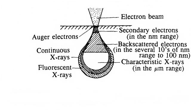
Electron Backscatter Diffraction (EBSD) is a widely used microscopy technique in material science. It analyzes the angles and phase differences of the backscattered electrons produced when a sample interacts with a high-energy electron beam to determine key characteristics such as crystal structure and grain orientation. Compared to a traditional Scanning Electron Microscope (SEM), EBSD provides higher spatial resolution and can obtain crystallographic data at the sub-micrometer level, offering unprecedented details for analyzing material microstructures.
Characteristics of the EBSD Technique
EBSD combines the microanalysis capabilities of Transmission Electron Microscope (TEM) and the large-area statistical analysis capabilities of X-ray diffraction. EBSD is known for its high-precision crystal structure analysis, fast data processing, simple sample preparation process, and the ability to combine crystallographic information with microstructural morphology in material science research. SEM equipped with an EBSD system not only provides micro-morphology and composition information but also enables microscopic orientation analysis, greatly facilitating the work of researchers.
Application of EBSD in SEM
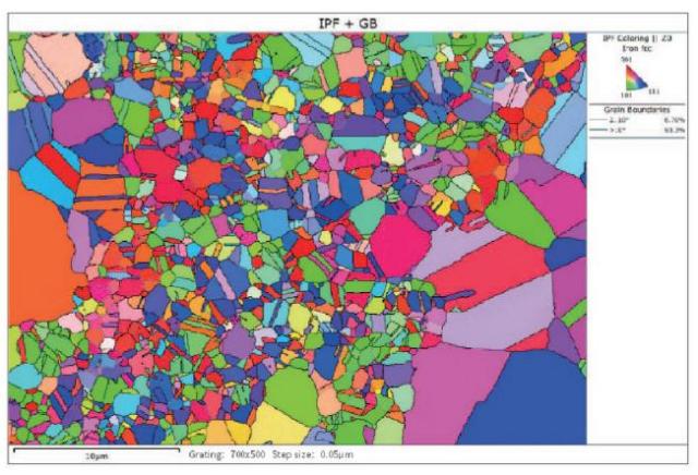
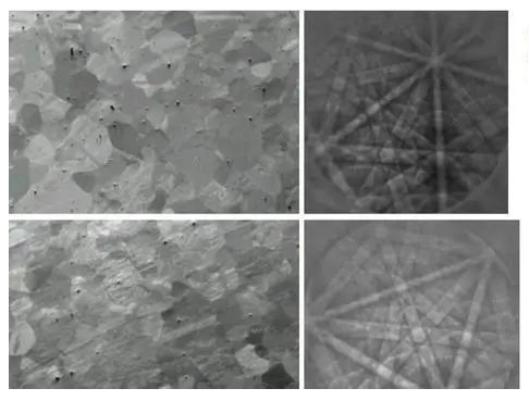
In SEM, when an electron beam interacts with the sample, various effects are generated, including the diffraction of electrons on regularly arranged crystal lattice planes. These diffractions form a "Kikuchi pattern," which not only contains information about the symmetry of the crystal system but also directly corresponds to the angle between crystal planes and crystallographic axes, with a direct relationship to the crystal system type and lattice parameters. This data can be used to identify crystal phases using the EBSD technique, and for known crystal phases, the orientation of the Kikuchi pattern directly corresponds to the orientation of the crystal.
EBSD System Components
To perform EBSD analysis, a set of equipment including a Scanning Electron Microscope and an EBSD system is required. The core of the system is the SEM, which produces a high-energy electron beam and focuses it on the sample surface. The hardware part of the EBSD system usually includes a sensitive CCD camera and an image processing system. The CCD camera is used to capture the backscattered electron images, and the image processing system is used to perform pattern averaging and background subtraction to extract clear Kikuchi patterns.
Operation of the EBSD Detector
Obtaining EBSD Kikuchi patterns in SEM is relatively simple. The sample is tilted at a high angle relative to the incident electron beam to enhance the backscattered signal, which is then received by a fluorescent screen connected to a CCD camera. The EBSD can be observed directly or after amplification and storage of the images. Software programs can calibrate the patterns to obtain crystallographic information. Modern EBSD systems can achieve high-speed measurements and can be used in conjunction with Energy-Dispersive X-ray Spectroscopy (EDS) probes to perform compositional analysis while rapidly obtaining sample orientation information.
Sample Preparation Principles
For effective EBSD analysis, sample preparation needs to follow certain principles, including the absence of residual stress, a flat surface (mechanical polishing), cleanliness, suitable shape and size, and good conductivity. The sample preparation process may involve ion etching, polishing, and other steps to ensure that the sample surface is suitable for EBSD analysis.
EBSD Calibration and Surface Scanning
Calibration is a critical step in the EBSD analysis process, ensuring an accurate correspondence between the Kikuchi patterns and crystallographic parameters. Surface scanning is another important application of EBSD technology, allowing researchers to perform extensive crystallographic analysis on the sample surface, thereby obtaining a comprehensive view of the material's microstructure.
