Common Misconceptions About SEM
A Scanning Electron Microscope (SEM) is a powerful microscope that uses a high-energy electron beam to scan the surface of a specimen, capturing signals emitted or scattered by electrons to generate high-resolution images of the specimen surface. SEM can magnify images by thousands to tens of thousands of times, revealing a microscopic world that is imperceptible to the naked eye.
Under the CIQTEK Scanning Electron Microscope, we can observe the fine textile structure of lizard skin cells, which allows for a visual examination of the structural characteristics of crystalline plates in the skin, such as their size, length, and arrangement. These images not only provide a visual feast but also offer crucial clues for scientists to interpret material properties, disease mechanisms, and biological tissue functions.
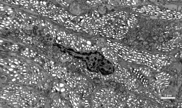
Figures1. Ultrastructure of lizard skin/30 kV/STEM
In the field of electron science, SEM helps engineers examine tiny solder joints and conductors on circuit boards in detail to ensure the precision and reliability of technology. In materials science, SEM can be used to analyze fracture surfaces of metal alloys, optimizing industrial design and processing technology. In biological applications, SEM can display the surface structure of bacteria and even observe interactions between viruses and host cells.
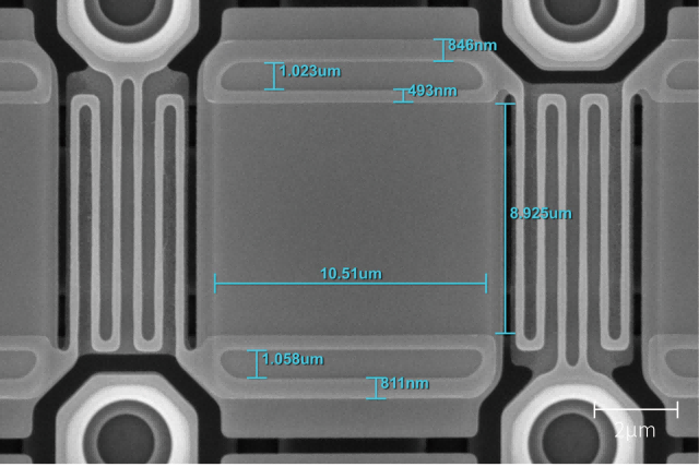
Figures2. SEM3200/Ordinary chip2/10 kV/ETD
SEM is not just a machine; it is more like a meticulous detective that helps us uncover the microscopic secrets in nature and man-made objects, providing strong support for scientific research and technological innovation. Through SEM, scientists can better understand the nature of materials, the structure of biological tissues, and the essence of various complex phenomena, pushing the boundaries of our knowledge forward.
Common Misconceptions about SEM:
1. Are SEM images in true colors?
SEM produces black and white images because they result from the interaction of electrons with the specimen, not from light waves. The colored SEM images typically seen are post-processed using digital coloring techniques to distinguish different structures or enhance visual effects.
2. Is higher magnification always better?
While SEM can provide extremely high magnification, not all research requires maximum magnification. Excessive magnification beyond the specimen's feature scale not only increases scanning time but may also lead to an increase in irrelevant information.
3. Can SEM see atoms?
Although SEM offers high resolution, it often cannot reach the level of observing individual atoms. To observe structures at the atomic scale, transmission electron microscopes (TEM) or scanning tunneling microscopes (STM) are typically needed.
4. Is SEM only suitable for solid and lifeless specimens?
While SEM was initially designed for solid materials, modern techniques allow observation of biological specimens as well. Through specific specimen treatments such as freezing, drying, or coating with conductive materials, SEM can also be used to observe biological tissues and cells.
5. Can SEM images fully represent the actual conditions of a specimen?
SEM images are two-dimensional projections obtained from specific angles and parameters, which may not fully reveal the three-dimensional structure and true conditions of the specimen. Additionally, the specimen preparation process may cause deformations or artifacts that can affect the accuracy of the results.