How Does Embedded Copper Coin Technology Enhance Thermal Management in High-Frequency PCBs?
How Does Embedded Copper Coin Technology Enhance Thermal Management in High-Frequency PCBs?
In the demanding world of high-frequency electronics, thermal management is not just a mechanical consideration—it is a critical factor that directly impacts electrical performance, signal integrity, and long-term reliability. As power densities increase in applications like 5G base stations and automotive radar, traditional cooling methods often fall short. This is where embedded copper coin technology emerges as a changing solution, offering a direct and highly efficient path for heat dissipation.
Here’s a detailed breakdown of how this technology enhances thermal management:
1. The Fundamental Principle: Creating a Low-Thermal-Resistance Path
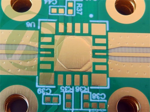
At its core, an embedded copper coin is a solid, thick piece of pure copper that is precision-machined and pressed into a milled cavity within the PCB's substrate during the lamination process. The key to its effectiveness lies in its ability to create a low-thermal-resistance pathway from the heat source to a heat sink or the opposite side of the board.
- Direct Thermal Connection: The coin is placed directly beneath a specific high-power component, such as a Power Amplifier (PA), Field-Programmable Gate Array (FPGA), or processor. This creates an intimate thermal connection, bypassing the insulating layers of the PCB laminate.
- Superior Thermal Conductivity: Copper has a thermal conductivity of approximately 400 W/mK, which is orders of magnitude higher than standard FR-4 (~0.3 W/mK) or evenhigh-frequency materials like M6. This massive disparity means heat is drawn away from the component and into the coin with remarkable efficiency.
2. Superiority Over Traditional Methods
To appreciate the copper coin's advantage, it's helpful to compare it to common alternatives:
- Vs. Thermal Vias: A cluster of thermal vias is a common solution. However, each via is a cylinder plated with a thin layer of copper (e.g., 20µm), filled with air or a thermal epoxy. The effective cross-sectional area of solid copper in a via field is relatively small. A solid copper coin, in contrast, provides a massive, uninterrupted cross-section of pure copper, resulting in significantly lower thermal resistance and much more efficient heat spreading.
- Vs. External Heat Sinks: While effective, top-side heat sinks can be bulky, heavy, and interfere with component placement or airflow. An embedded coin can often reduce the size and weight of an external heat sink or, in some cases, eliminate the need for one altogether, enabling more compact and elegant designs.

3. Direct Benefits for High-Frequency Performance
The thermal benefits of the copper coin translate directly into enhanced electrical performance, which is crucial for high-frequency PCBs:
- Preventing Performance Drift: Many active components, especially RF components, have performance parameters (like gain, output power, and noise figure) that are sensitive to temperature. By maintaining a stable, lower operating temperature (Tj, junction temperature), the copper coin ensures the component performs consistently within its specified range.
- Improving Signal Integrity: Excessive heat can increase the dissipation factor (Df) of the PCB laminate and alter its dielectric constant (Dk). This can lead to signal attenuation, impedance mismatches, and phase shifts. Effective cooling via a copper coin helps maintain the stable electrical properties of the surrounding M6 material or IT-180 material.
- Enabling Higher Power Density: By efficiently managing the "hotspots," designers can safely use more powerful components or pack them more densely on the board without fear of thermal throttling or failure, pushing the boundaries of what's possible in a given form factor.
4. Enhancing Mechanical Reliability and Lifespan
Thermal cycling—the repeated heating and cooling of a board during operation—is a primary cause of failure in electronics.
- Reduced Thermal Stress: By effectively dissipating heat, the copper coin minimizes the peak temperature and the temperature delta across the board and within the component itself. This reduces the mechanical stress on solder joints and the PCB laminate, preventing cracking and delamination.
- Increased Mean Time Between Failures (MTBF): A cornerstone of reliability engineering is that component failure rates decrease exponentially with lower operating temperatures. By keeping critical components cool, the embedded copper coin directly contributes to a longer, more reliable operational lifespan for the entire system.
Implementation in a Hybrid PCB
In a sophisticated board like the Copper Coin Embedded 6-Layer M6 IT180 Hybrid PCB, the coin is strategically placed in the center of the PCB stackup. It connects directly from the component on the outer layer down to the internal ground planes or to the bottom side, where it can be attached to an external chassis or heat spreader. This integration is seamless and is completed during lamination, ensuring a robust mechanical bond and optimal thermal transfer without compromising the board's structural integrity.
Conclusion
Embedded copper coin PCB technology is a powerful and targeted thermal management solution that directly addresses the thermal bottlenecks in high-frequency, high-power PCBs. It moves beyond the limitations of traditional vias and heat sinks by providing a low-resistance, high-conductivity thermal highway. The result is not just a cooler-running board, but one that delivers superior electrical performance, greater design flexibility, and unparalleled long-term reliability—making it an indispensable technology for next-generation applications in 5G, automotive, and aerospace.
