\"Nature Materials | Visualizing Graphene Magnetism CIQTEK SNVM Enables a Key Breakthrough in Graphene Spintronics\
A research team led by Prof. Haomin Wang from the Shanghai Institute of Microsystem and Information Technology, Chinese Academy of Sciences, has achieved significant progress in studying the magnetism of zigzag graphene nanoribbons (zGNRs) using the CIQTEK Scanning NV Microscope (SNVM).
Building on their previous research, the team fabricated oriented atomic grooves in hexagonal boron nitride (hBN) by pre-etching with metal nanoparticles and synthesized chiral-controlled graphene nanoribbons within these grooves through a vapor-phase catalytic CVD method. The resulting ~9 nm-wide zGNRs embedded in the hBN lattice exhibited intrinsic magnetic properties, which were directly confirmed experimentally for the first time using SNVM combined with magnetic transport measurements.
This groundbreaking work lays a solid foundation for developing graphene-based spintronic devices. The study, titled “Signatures of magnetism in zigzag graphene nanoribbons embedded in a hexagonal boron nitride lattice”, was published in the renowned journal Nature Materials.
 https://doi.org/10.1038/s41563-025-02317-4
Understanding Graphene Magnetism
Graphene, as a unique two-dimensional material, exhibits p-orbital electron magnetism that differs fundamentally from the localized d/f orbital magnetism found in conventional materials. This distinction opens new directions for exploring carbon-based quantum magnetism. Zigzag graphene nanoribbons (zGNRs) are particularly promising for spintronic applications because of their predicted magnetic electronic states near the Fermi level. However, detecting zGNR magnetism through electrical transport measurements has remained highly challenging.
The main difficulties include the limited length of bottom-up synthesized nanoribbons, which complicates device fabrication, and the chemically reactive edges that lead to instability or inhomogeneous doping. Furthermore, in narrow zGNRs, strong antiferromagnetic coupling between edge states makes it difficult to electrically detect magnetic signals. These challenges have hindered direct observation of intrinsic magnetism in zGNRs.
SNVM Reveals Magnetic Signals at Room Temperature
Embedding zGNRs within an hBN lattice enhances edge stability and introduces built-in electric fields, providing an ideal environment for studying magnetism. Using CIQTEK’s room-temperature SNVM, the researchers directly visualized magnetic signals in zGNRs for the first time under ambient conditions.
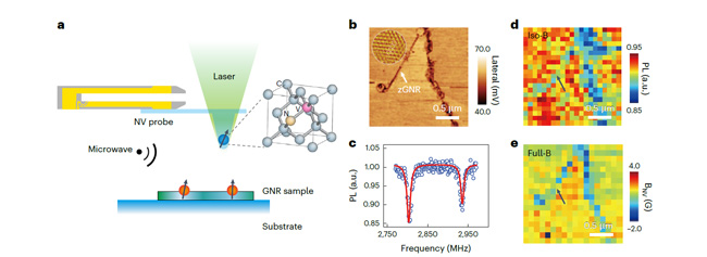
Figure 1. Magnetic measurement of zGNRs embedded in a hexagonal boron nitride lattice using the Scanning NV Microscope
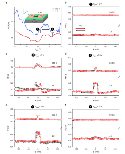
In electrical transport measurements, the ~9 nm-wide zGNR transistors demonstrated high conductivity and ballistic transport behavior. Under magnetic fields, the devices showed pronounced anisotropic magnetoresistance, with resistance changes up to 175 Ω and a magnetoresistance ratio of approximately 1.3% at 4 K, which persisted up to 350 K. Magnetic hysteresis appeared only when the magnetic field was applied perpendicular to the zGNR plane, confirming magnetic anisotropy. Analysis of the angular dependence of magnetoresistance indicated that the magnetic moments were oriented normal to the sample surface. The decrease in magnetoresistance with increasing source-drain bias and temperature revealed interactions between magnetic response, charge transport, and thermal vibrations.
By combining SNVM imaging with transport characterization, this study provides the first direct evidence of intrinsic magnetism in zGNRs embedded in hBN and demonstrates the potential for electric-field control of magnetic behavior. This work deepens the understanding of graphene magnetism and opens new opportunities for developing graphene-based spintronic devices.
Experience Nanoscale Magnetic Imaging with CIQTEK SNVM
CIQTEK invites researchers to experience the Scanning NV Microscope (SNVM), a world-leading nanoscale magnetic imaging system featuring a temperature range of 1.8–300 K, a 9/1/1 T vector magnetic field, 10 nm magnetic spatial resolution, and 2 μT/Hz¹ᐟ² magnetic sensitivity.
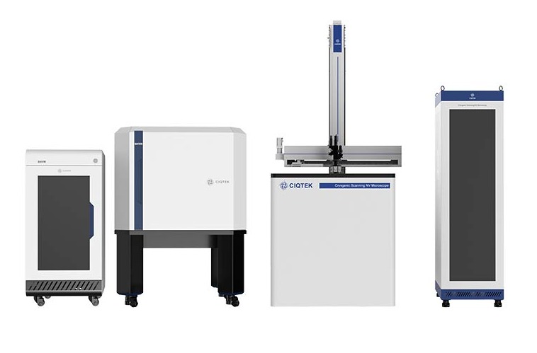 CIQTEK SNVM: the ambient version and the cryogenic version
The SNVM integrates diamond nitrogen-vacancy (NV) center-based optically detected magnetic resonance (ODMR) with atomic force microscopy (AFM) scanning technology. It offers high spatial resolution, superior magnetic sensitivity, multifunctional detection, and non-invasive imaging capabilities, making it an essential tool for research in magnetic domain characterization, antiferromagnetic imaging, superconductivity studies, and two-dimensional magnetic materials.
