What Makes TMM13i High Frequency PCBs Ideal for Demanding RF and Microwave Applications?


In the world of high-frequency electronics, the choice of printed circuit board (PCB) material is critical to achieving optimal performance and reliability. Rogers Corporation’s TMM13i isotropic thermoset microwave material stands out as an exceptional choice for high-frequency applications. This ceramic thermoset polymer composite is specifically engineered to deliver high reliability in plated through-hole strip-line and micro-strip configurations. By combining the beneficial properties of both ceramic and PTFE substrates, Rogers TMM13i allows designers to leverage the processing ease of soft substrate materials without compromising on electrical or thermal performance.


TMM13i features


One of the key features of TMM13i laminate is their exceptionally low thermal coefficient of dielectric constant, rated at -70 ppm/°C. This ensures remarkable stability of the dielectric constant across a broad temperature spectrum, making it an excellent candidate for applications subject to significant temperature variations. Such thermal stability is essential in environments where performance consistency cannot be compromised.


Moreover, TMM13i PCB exhibits isotropic coefficients of thermal expansion (CTE)—19 ppm/°C in the X and Y axes, and 20 ppm/°C in the Z direction. These values are closely matched to those of copper, which significantly enhances the reliability of plated through holes and reduces etch shrinkage. This CTE matching minimizes the risk of delamination or cracking under thermal stress, thereby extending the lifecycle of the assembled PCB.


Another advantage of TMM13i substrate is its high dielectric constant of 12.85±0.35. This property allows for considerable miniaturization of circuit components, supporting the trend toward more compact and integrated electronic devices. In addition, the material’s low dissipation factor of 0.0019 at 10 GHz ensures minimal signal loss and improved energy efficiency, which is particularly valuable in high-speed digital and RF microwave circuits.


Our PCB Manufacturing Capabilities with TMM13i Material


PCB Manufacturing Capabilities with TMM13i Material


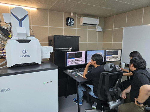
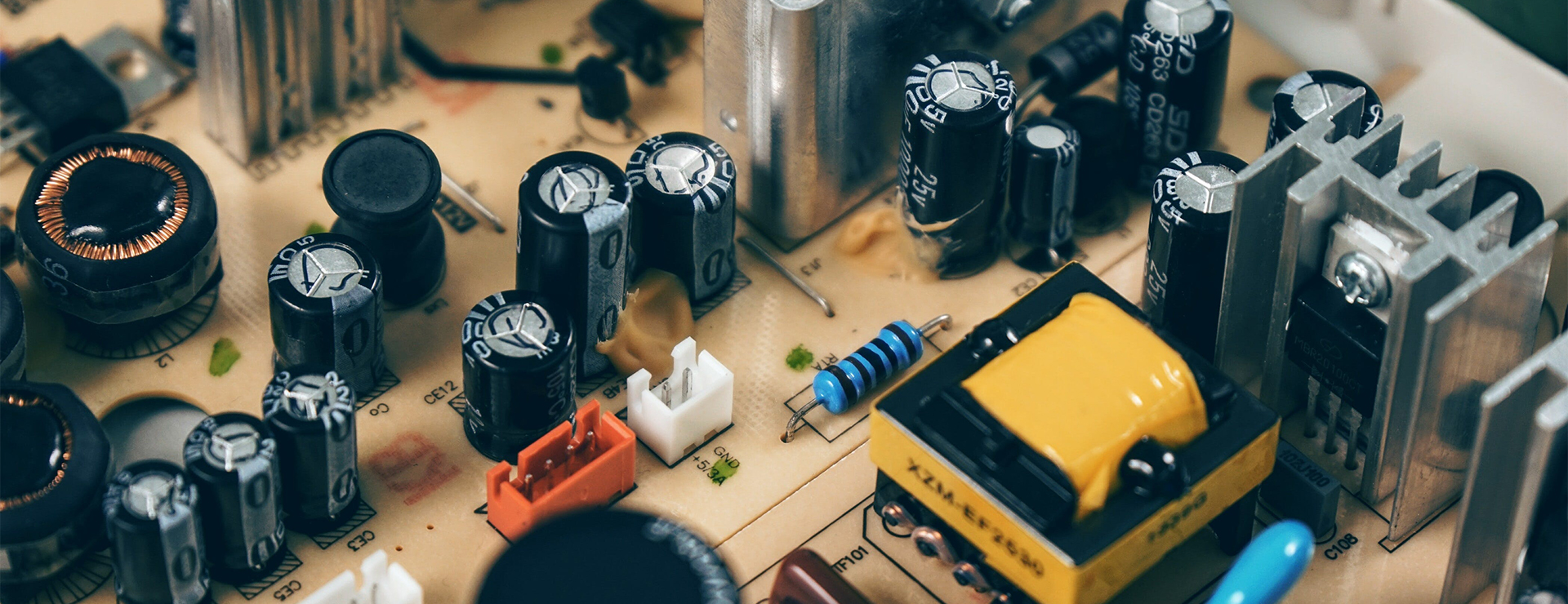
We take pride in offering advanced PCB fabrication services utilizing Rogers TMM13i high-frequency laminates. Our manufacturing facilities support a wide variety of PCB configurations—including single-layer, double-layer, multilayer, and hybrid boards—to meet diverse and customized project requirements.


We provide flexible copper weight options, including 1 oz (35 µm) and 2 oz (70 µm), to address specific conductivity and current-carrying needs. Our processes also support multiple dielectric thicknesses, from 15 mil (0.381 mm) up to 500 mil (12.7 mm), accommodating both standard and high-power designs.


For larger format designs, we can produce PCBs with dimensions up to 400 mm x 500 mm. Additionally, we offer a variety of solder mask colors—such as green, black, blue, yellow, and red—enabling alignment with your aesthetic branding or functional identification requirements.


To ensure superior performance and longevity, we provide a comprehensive selection of surface finishes: bare copper, HASL (Hot Air Solder Leveling), ENIG (Electroless Nickel Immersion Gold), OSP (Organic Solderability Preservative), immersion tin, immersion silver, ENEPIG (Electroless Nickel Electroless Palladium Immersion Gold), and pure gold.


TMM13i High Frequency PCBs


Applications of TMM13i High Frequency PCBs


TMM13i-based PCBs are ideally suited for a broad range of high-performance applications. These include chip testers, dielectric polarizers, lenses, filters, couplers, and various RF and microwave circuits. Their excellent electrical properties also make them a preferred material in satellite communication systems, where signal integrity and thermal stability are paramount.


Whether you are designing advanced aerospace systems, telecommunications infrastructure, or sophisticated test and measurement equipment,TMM13i High Frequency PCBs provide the reliability and performance needed to succeed in demanding environments.


Why is TLX-9 the Preferred High-Frequency Laminate for Demanding Aerospace and Telecom Systems?


In the rapidly advancing world of high-frequency electronics, the choice of printed circuit board (PCB) material is critical to the performance, reliability, and efficiency of the end product. Taconic’s TLX-9 high-frequency PCB material stands at the forefront of this innovation, offering an exceptional blend of electrical, mechanical, and thermal characteristics tailored for demanding applications. This article delves into the core attributes, capabilities, and uses of TLX-9, illustrating why it is a top-tier choice for engineers and designers in industries where precision and performance are non-negotiable.


An Introduction to TLX-9 High Frequency Material

TLX-9 is a premium-gradehigh-frequency laminate constructed from a polytetrafluoroethylene (PTFE) base reinforced with woven fiberglass. This sophisticated composite represents a significant achievement in copper-clad PTFE technology, merging outstanding high-frequency electrical properties with excellent mechanical durability. It is manufactured under strict controls to ensure consistent performance, making it ideal for applications where signal integrity and operational stability are paramount.


Moreover, Taconic TLX-9 complies with the UL 94 V-0 flammability standard, enhancing its suitability for safety-sensitive environments. The material is also compatible with standard PCB fabrication processes—including shearing, drilling, milling, and plating—enabling straightforward integration into existing production workflows without the need for specialized equipment or techniques.


Key Features and Technical Specifications

The superior performance of TLX-9 PCB stems from its carefully engineered properties:


TLX-9 PCB features


1) Dielectric Constant (Dk): At 10 GHz, the dielectric constant is 2.50, offering exceptional signal stability and reduced propagation delay, which is crucial for high-speed and high-frequency circuit operation.


2) Dissipation Factor (Df): With an ultra-low dissipation factor of 0.0019 at 10 GHz, TLX-9 minimizes signal loss, thereby enhancing the efficiency of power transmission and preserving signal clarity in RF and microwave applications.


3) Moisture Absorption: Boasting a moisture absorption rate of less than 0.02%, TLX-9 maintains consistent performance even under high-humidity conditions, ensuring long-term reliability and reducing the risk of degradation.


4) Dielectric Strength: The material offers a dielectric breakdown strength exceeding 60 kV, making it highly suitable for high-power and high-voltage applications such as radar systems and microwave amplifiers.


5) Resistivity: TLX-9 exhibits high volume and surface resistivity, both rated at 10⁷MΩ/cm and MΩrespectively, providing superior insulation resistance and minimizing current leakage.


6) Peel Strength: The laminate demonstrates strong bond integrity, with a peel strength of 12.0 lbs per linear inch for 1 oz copper, ensuring that copper layers remain securely attached throughout the assembly process and product lifecycle.


7) Thermal Expansion: The coefficient of thermal expansion (CTE) is tightly controlled, with X-Y CTE values of 9–12 ppm/°C and Z-axis CTE ranging from 130–145 ppm/°C. This dimensional stability across temperatures prevents deformation and supports the structural integrity of multilayer and high-density designs.


PCB Fabrication Capabilities with TLX-9


PCB Fabrication Capabilities with TLX-9


TLX-9 substrate supports a wide range of PCB configurations, including single-sided, double-sided, multilayer, and hybrid constructions. Available in thicknesses of 5, 10, 20, and 30 mils, it provides flexibility for various design requirements. The finished copper weight can be specified as 1 oz or 2 oz, supporting both fine-line tracing and higher current carrying capacity.


The maximum panel size available is 400 mm x 500 mm, accommodating both large-format boards and multi-design panelization. A variety of solder mask colors are offered, including green, black, blue, red, and yellow. Surface finish options include immersion gold (ENIG), hot air solder leveling (HASL), immersion silver, immersion tin, bare copper, OSP, electroplated gold, and ENEPIG, providing ample choices based on application needs and assembly conditions.


TLX-9 Taconic RF PCBs


Typical Applications

TLX-9 Taconic RF PCBs are widely used in advanced electronic systems where high reliability and signal fidelity are essential. Common applications include:


  • Low Noise Amplifiers (LNA)
  • Low Noise Block Converters (LNB)
  • Low Noise Converters (LNC)
  • Large-format antenna systems for Personal Communication Services (PCS) and Personal Communication Networks (PCN)
  • High Power Amplifiers


These applications benefit from the material’s stable electrical properties, low loss characteristics, and robust construction, making TLX-9 Taconic High Frequency PCB a preferred substrate in aerospace, military, telecommunications, and other high-performance sectors.


Conclusion

TLX-9 Taconic RF PCB Circuit Board combines cutting-edge material science with practical manufacturability, offering a reliable solution for the most challenging high-frequency designs. Its balanced performance across electrical, thermal, and mechanical domains ensures that it meets the rigorous demands of modern RF and microwave applications. Whether for consumer communication devices or mission-critical aerospace systems, TLX-9Taconic PCB Substrate delivers consistent quality and superior performance, establishing itself as a material of choice among engineers and designers worldwide.


Why Should You Choose DiClad 870 for Your High-Frequency and Low-Loss PCB Designs?


In the world of high-frequency electronics, the choice of printed circuit board material is critical to achieving optimal performance and reliability. Rogers DiClad 870 stands out as an exceptional high-frequency laminate, specifically engineered to meet the rigorous demands of advanced RF and microwave applications. This woven fiberglass-reinforced, PTFE-based composite delivers superior electrical properties, dimensional stability, and mechanical durability—making it an ideal substrate for high-speed digital and analog designs.


One of the key advantages of Rogers DiClad 870 is its unique construction. By utilizing a higher proportion of PTFE content and fewer plies of woven fiberglass, it achieves a lower dielectric constant and exceptionally low dissipation factor. What sets it apart from non-woven PTFE laminates is its enhanced dimensional stability, thanks to the strategic alignment of coated fiberglass plies in the same direction. This structural integrity ensures consistent performance even under varying operational conditions.


Key Features of DiClad 870 High Frequency Laminates


Features of DiClad 870


1) Stable Dielectric Constant: DiClad 870 maintains a consistent dielectric constant of 2.33 across a broad frequency spectrum—from 1 MHz all the way up to 10 GHz. This uniformity ensures reliable signal transmission with minimal phase distortion, making it suitable for high-speed and high-frequency designs.


2) Low Dissipation Factor: With an ultra-low dissipation factor of just 0.0013 at 10 GHz, these laminates significantly reduce signal loss, preserve energy efficiency, and enhance signal integrity—especially crucial in sensitive RF and microwave circuits.


3) Excellent Copper Adhesion: The laminate demonstrates outstanding copper peel strength, measuring 14 lbs/in when tested with 35μm foil per IPC TM-650 2.4.8. This strong bond between copper and substrate ensures long-term reliability and reduces the risk of delamination.


4) Minimal Moisture Absorption: DiClad 870’s moisture absorption rate is an impressively low 0.02%, allowing it to perform reliably in humid or challenging environments without compromising electrical properties.


5) High Flame Resistance: Complying with UL 94-V0 standards, this material offers excellent flammability resistance, contributing to safer end-products and compliance with international safety regulations.


PCB Manufacturing Capabilities with DiClad 870

We provide comprehensive manufacturing solutions for DiClad 870 PCBs, supporting a wide range of design requirements:


PCB Manufacturing Capabilities with DiClad 870


Layer Configurations: From single and double-sided boards to complex multi-layer and hybrid stack-ups, we accommodate diverse project needs with precision.


Dielectric Thickness Options: Choose from standard thicknesses including 31mil (0.787mm), 93mil (2.286mm), and 125mil (3.175mm) to meet specific impedance and mechanical requirements.


Copper Weights: Available in 1oz (35µm) and 2oz (70µm) options, providing flexibility in current carrying capacity and thermal management.


Panel Size: We support PCB dimensions up to 400mm x 500mm, ideal for both large single-board layouts and multi-design panelization.


Solder Mask Varieties: Customize the appearance of your boards with a selection of solder mask colors including Green, Black, Blue, Red, Yellow, and more.


Surface Finishes: Our offerings include Immersion Gold (ENIG), HASL, Immersion Silver, Immersion Tin, Bare Copper, OSP, ENEPIG, and Pure Gold, giving you the flexibility to choose based on solderability, durability, and application environment.


DiClad 870high frequency PCB


Typical Applications

DiClad 870 substrates are widely used in applications where consistent dielectric properties and low loss are essential. Common uses include:


  • RF components such as filters, couplers, and low-noise amplifiers
  • Power dividers and combiners in telecommunications infrastructure
  • Base station antennas and signal distribution networks
  • Radar feed networks, commercial phased array systems, and aerospace guidance systems
  • Digital radio antennas and other high-frequency communication devices


Whether you are designing for aerospace, defense, telecom, or high-performance computing, DiClad 870high frequency PCB offers a reliable foundation for building circuits that demand tight impedance control, minimal signal loss, and unwavering performance.


In today’s fast-paced world, keeping track of your health and staying connected is more important than ever. The ET458 Smartwatch offers a perfect blend of advanced technology, stylish design, and practical daily features. With its 1.56-inch AMOLED HD screen, every detail is crisp and colorful, making notifications, fitness data, and watch faces a joy to view.


The ET458 is more than just a smartwatch – it’s your personal health assistant. Featuring ECG detection, one-touch micro-physical examination, and continuous monitoring of heart rate, blood oxygen, and sleep patterns, it helps you understand your body like never before. Emotional fatigue detection allows you to stay aware of stress levels, giving you the tools to manage both physical and mental wellness.


For those with an active lifestyle, the ET458 supports multiple sports modes, while IP68 waterproofing and a long-lasting 380mAh battery ensure it keeps up with your adventures. Its ultra-bright flashlight with four modes – constant light, night running, warning, and SOS – adds an extra layer of safety and convenience.


The ET458 also excels in smart connectivity. With Bluetooth calling, NFC access control, and Alipay payment, you can handle daily tasks effortlessly from your wrist. Plus, the vast online watch face library allows you to personalize your watch to match your style.


Whether you’re focused on fitness, wellness, or staying connected on the go, the ET458 Smartwatch combines elegance, durability, and advanced health features. It’s not just a watch – it’s a comprehensive companion for modern life.

OEM ODM Smartwatch Manufacturing Services

In the fields of life sciences, biomedicine, food inspection, and soft matter research, achieving high-resolution imaging of hydrated and beam-sensitive samples has always been a major challenge. Conventional sample preparation methods, such as chemical fixation, dehydration, and drying, often result in shrinkage, deformation, or structural damage, leading to results that deviate from the true state of the sample.


Leveraging its advanced scanning electron microscopy technology, CIQTEK has introduced the Cryo-SEM Solution, which integrates low-temperature freezing and vacuum transfer. This enables in-situ, non-destructive, and high-fidelity microscopic observation of biological and sensitive samples, truly “freezing” the microscopic details of life.


With liquid-nitrogen slush rapid-freezing technology, samples can be vitrified instantly at -210 °C, preserving their original morphology and chemical composition to the greatest extent. The integrated cryo-preparation system combines freeze-fracture, sublimation coating, and low-temperature transfer, avoiding the complexity and potential errors of conventional manual preparation. Throughout the entire process, samples are maintained under cryogenic vacuum conditions and transferred to the SEM cryo-stage, where high-resolution imaging at -180 °C effectively suppresses electron beam damage and significantly improves image quality.


Cryo-prepared boxwood leaf showing intact vein structures, while the untreated sample exhibits severe shrinkage.

Cryo-prepared boxwood leaf showing intact vein structures, while the untreated sample exhibits severe shrinkage.


Yogurt

Cryo-prepared yogurt sample clearly reveals protein networks and fungal hyphae.


Mold

Cryo-prepared yogurt sample clearly reveals protein networks and fungal hyphae.

Cryo-prepared yogurt sample clearly reveals protein networks and fungal hyphae.


In addition, the system offers strong compatibility, adaptable across CIQTEK's full range of SEMs and dual-beam FIBSEM systems, meeting diverse needs from routine observation to advanced analysis.


The CIQTEK Cryo-SEM Solution is more than just a set of instruments. It embodies a scientific approach dedicated to faithfully restoring the microscopic world. It empowers researchers to overcome technical limitations, capture critical details at the micro scale of life, and drive both fundamental research and applied development to new heights.


September 26–30, Wuhan

At the 2025 Chinese Electron Microscopy Academic Conference, CIQTEK will unveil eight cutting-edge EM solutions.

Stay tuned!

CIQTEK is pleased to announce the successful installation and training of the FIBSEM DB550 at our Korean distributor GSEM’s Electron Microscope Center. This milestone marks an important step in expanding access to advanced focused ion beam scanning electron microscope (FIBSEM) technology in South Korea.


CIQTEK FIBSEM DB550 Now Operational at GSEM Electron Microscope Center in South Korea


The DB550 combines high-resolution imaging with precise ion beam milling, enabling researchers to perform 3D reconstruction, cross-sectional analysis, and nanoscale material modification with efficiency and accuracy. With these capabilities, the system opens new possibilities for semiconductor analysis, materials science, and life science research.

Following installation, CIQTEK engineers provided hands-on training to the GSEM team, covering both standard workflows and advanced applications. The interactive sessions ensured that users gained practical experience in operating the instrument, from sample preparation to high-resolution imaging and data analysis. The enthusiasm and engagement of the GSEM team highlighted the strong potential for the DB550 to support diverse research projects at the center.


CIQTEK FIBSEM DB550 Now Operational at GSEM Electron Microscope Center in South Korea


This collaboration reflects CIQTEK’s commitment to working closely with partners worldwide. By equipping GSEM’s facility with the DB550, we are not only strengthening our presence in the Korean market but also helping local researchers gain access to cutting-edge tools for scientific innovation.

We look forward to seeing the exciting results that GSEM’s Electron Microscope Center will achieve with the DB550, and we remain committed to providing ongoing technical support and collaboration.


CIQTEK FIBSEM DB550 Now Operational at GSEM Electron Microscope Center in South Korea

For adventure enthusiasts who demand both durability and functionality, the HT36 smartwatch delivers exceptional performance in any environment. Its robust construction features 6H hardened glass and 3ATM waterproof rating, making it equally suited for mountain trails and urban exploration. The brilliant 2.01-inch HD display remains perfectly visible even in direct sunlight, while the innovative rotating crown provides satisfying tactile feedback for effortless navigation through menus and features.


What truly sets the HT36 apart is its exceptional positioning capabilities. Supporting six global satellite systems including GPS, GLONASS, and Beidou, it maintains accurate tracking even in challenging urban canyons or remote wilderness areas. The built-in environmental sensors provide crucial real-time data including altitude, barometric pressure, and compass direction - essential information for any serious outdoor adventure. Beyond its navigation prowess, the watch offers comprehensive health monitoring with 24/7 heart rate tracking, blood oxygen measurement, and sleep quality analysis.


The massive 540mAh battery ensures weeks of typical usage between charges, while practical features like wireless calling, music control, and weather updates keep you connected wherever your adventures take you. With over 100 sports modes and a built-in flashlight for nighttime safety, the HT36 proves that you don't need to sacrifice functionality for durability in a outdoor smartwatch.

How Does Rogers TMM10 PCB Material Enhance Thermal and Electrical Performance?


In the demanding world of high-frequency electronics, the choice of printed circuit board (PCB) substrate is paramount to the success of any application. Rogers Corporation's TMM10  microwave materials stand out as a superior solution, engineered to meet the rigorous requirements of modern RF and microwave circuits. This ceramic thermoset polymer composite is specifically designed for high plated-through-hole (PTH) reliability in both stripline and microstrip configurations, offering a unique blend of electrical and mechanical properties that bridge the gap between traditional materials.


Superior Material Properties for Enhanced Performance


The TMM10 substrate is celebrated for its exceptional electrical characteristics, which directly contribute to more efficient and compact circuit designs. It boasts a stable dielectric constant (Dk) of 9.20 with a tight tolerance of±0.23. This high and consistent Dk is a significant advantage for designers aiming to minimize the physical size of components like antennas and filters, enabling substantial miniaturization without compromising performance.


TMM10's features


A critical factor in high-frequency applications is signal integrity, which is safeguarded by TMM10's remarkably low dissipation factor of 0.0022 at 10 GHz. This minimal loss tangent ensures that signal loss is drastically reduced, leading to enhanced efficiency and superior performance in power-sensitive applications. Furthermore, the thermal coefficient of dielectric constant (-38 ppm/°K) guarantees outstanding electrical stability across a wide range of operating temperatures, making it reliable in environments subject to thermal fluctuations.


TheTMM10 PCBmaterial’s mechanical and thermal properties are equally impressive. With a coefficient of thermal expansion (CTE) of 21 ppm/°K on the X and Y axes and 20 ppm/°K on the Z-axis, TMM10 closely matches the CTE of copper. This compatibility is crucial for producing highly reliable plated through-holes, preventing barrel cracking and ensuring long-term structural integrity. Additionally, its thermal conductivity of 0.76 W/m/K is approximately double that of standard PTFE/ceramic laminates, significantly improving heat dissipation and helping to manage thermal loads in power-amplifier and other heat-sensitive applications. The robust mechanical properties also effectively resist creep and cold flow, ensuring dimensional stability and durability under stress.


Advanced PCB Manufacturing Capabilities with TMM10

PCB Manufacturing Capabilities with TMM10


At Bicheng, we leverage our advanced manufacturing expertise to fully harness the potential of Rogers TMM10 laminates. We provide comprehensive PCB solutions tailored to diverse and complex project requirements. Our capabilities include the production of:


1)Layer Variations: Single-layer, double-layer, multilayer, and hybrid PCB constructions, offering design flexibility for various circuit complexities.


2)Copper Weights: Standard options of 1oz (35µm) and 2oz (70µm) to cater to different current-carrying and thermal management needs.


3)Board Thickness: A wide range from a slender 15mil (0.381mm) to a substantial 500mil (12.70mm), supporting everything from ultra-compact to extremely robust and durable designs.


4)Panel Size: Capable of handling large formats up to 400mm x 500mm, ideal for sizable projects and efficient panelization.


5)Aesthetics and Finish: A selection of solder mask colors (green, black, blue, yellow, red) and a variety of surface finishes including Bare Copper, HASL, ENIG, Immersion Silver, Immersion Tin, ENEPIG, Pure Gold, and OSP to meet both technical and aesthetic specifications.


Rogers TMM10 PCB


Diverse Application Spectrum

The exceptional properties of TMM10 PCBs make them the material of choice for a wide array of high-performance applications. They are commonly deployed in:


1)Chip Testers: Where signal integrity and thermal stability are critical for accurate testing.


2)Dielectric Polarizers and Patch Antennas: Benefiting from the stable high Dk for compact, efficient design.


3)Satellite Communication Systems and GPS Antennas: Where low signal loss and reliability under varying environmental conditions are non-negotiable.


Conclusion

Rogers TMM10 represents a paradigm shift in high-frequency PCB materials, combining the best attributes of ceramics and polymers without their inherent limitations. For engineers designing next-generation RF and microwave products, TMM10 offers a path to miniaturization, enhanced reliability, and superior electrical performance. As a trusted PCB supplier, Bicheng possesses the technical proficiency to transform this advanced material into high-quality, reliable circuit boards that meet your most challenging application demands.


Contact us today to discuss how we can support your specific project needs with our TMM10 high frequency PCB capabilities.