In the use of smart sports watches, users often face some frustrating issues:

  • GPS drift: running tracks appear inaccurate or offset;
  • Unstable Bluetooth: frequent disconnections with phones or earbuds;
  • High power consumption: battery drains too fast, limiting usage time.

These problems are not solely caused by software. A key factor lies in the crystal oscillator (XO) selection during hardware design.

Crystal Oscillator Solutions for Sports Watches

The Role of Crystal Oscillators

Crystal oscillators serve as the precise clock source for the GPS module, Bluetooth chip, and MCU controller inside sports watches.

  • For GPS: even a tiny clock error can lead to significant location drift.
  • For Bluetooth: frequency deviation may cause connection loss or data errors.
  • For power management: unstable clocks reduce efficiency in low-power modes, draining the battery faster.

Root Causes of Common Issues

  1. Low-accuracy oscillators → large temperature drift, poor stability in varying environments
  2. Insufficient power optimization → faster battery drain.
  3. Lack of differential/temperature-compensated solutions → poor performance in outdoor environments.

JGHC Crystal Oscillator Solutions

For sports watches and wearable devices, JGHC recommends:

Conclusion


When your sports watch suffers from inaccurate GPS, unstable Bluetooth, or short battery life, the true reason might be that the wrong crystal oscillator was chosen.

JGHC Crystals is committed to providing high-precision, low-power, and highly reliable oscillator solutions for wearable devices, helping brands deliver superior user experiences.


For more crystal oscillator application solutions, please contact JGHC.

The basic working principle of quartz crystal oscillator

Quartz crystal oscillators utilize high-quality piezoelectric crystals, harnessing the piezoelectric effect to generate stable oscillations. The crystal's quality factor (Q) directly impacts frequency stability—a higher Q provides a more accurate and reliable clock signal. The vibration frequency characteristics are determined by three key factors: crystal thickness, crystal geometry, and cutting method.


Effect of thickness on frequency

The frequency of a quartz crystal is inversely proportional to the thickness of the crystal:

Thin wafers: Support higher oscillation frequencies, ideal for high-frequency applications.

Thick wafers: small vibration amplitude and excellent resistance to mechanical shock

Technological breakthrough : Overtone crystal technology enables a chip with a fundamental frequency of 20MHz to reach 100MHz through the fifth overtone, allowing medium and low fundamental frequency chips to meet high-frequency requirements of hundreds of megahertz.


Chip shape and frequency characteristics


Tuning Fork Chip

Typical application: 32.768kHz crystal oscillator

Typical dimensions: 3.2 × 1.5 × 0.8 mm

Temperature characteristics: parabolic characteristics of -0.04ppm/℃²

Manufacturing process: Photolithography technology is used to achieve micron-level precision

Frequency determining factors: mainly depends on the fork length (L), the longer the length, the higher the frequency

Advantages: Especially suitable for low-frequency precise timing scenarios


Fectangular Wafer

Frequency range: MHz level application

Miniaturization: From 7.0×5.0mm to 1.6×1.2mm

High frequency: Up to 300MHz through chamfered edge technology

Low power consumption: current consumption can be as low as 0.5μA

Main features: convenient for large-scale production and standardized packaging

Frequency Determinants: Thickness is the Main Influencing Factor


Comparison of key cutting technologies

The cutting angle of the quartz crystal (defined in the XYZ coordinate system) directly affects:

(1) Long-term aging characteristics

(2) Temperature stability

(3) Frequency accuracy

Mainstream cutting methods : AT cutting, BT cutting, SC cutting, IT cutting, and special cutting processes designed specifically for tuning fork wafers. Each method has its own performance advantages and applicable scenarios.


Contact

Need the optimal quartz crystal oscillator solution for your application? Our team of engineers can provide complete crystal oscillator selection recommendations and technical support, from low to high frequencies, based on your specific application needs.

Please contact our sales team:  

Tel: 0086-576-89808609  

Email: market@acrystals.com

Website: [www.acrystals.com](http://www.acrystals.com)  

What Makes Rogers RT/duroid 5870 Laminates Ideal for High-Frequency Electronics and Precision Circuits?


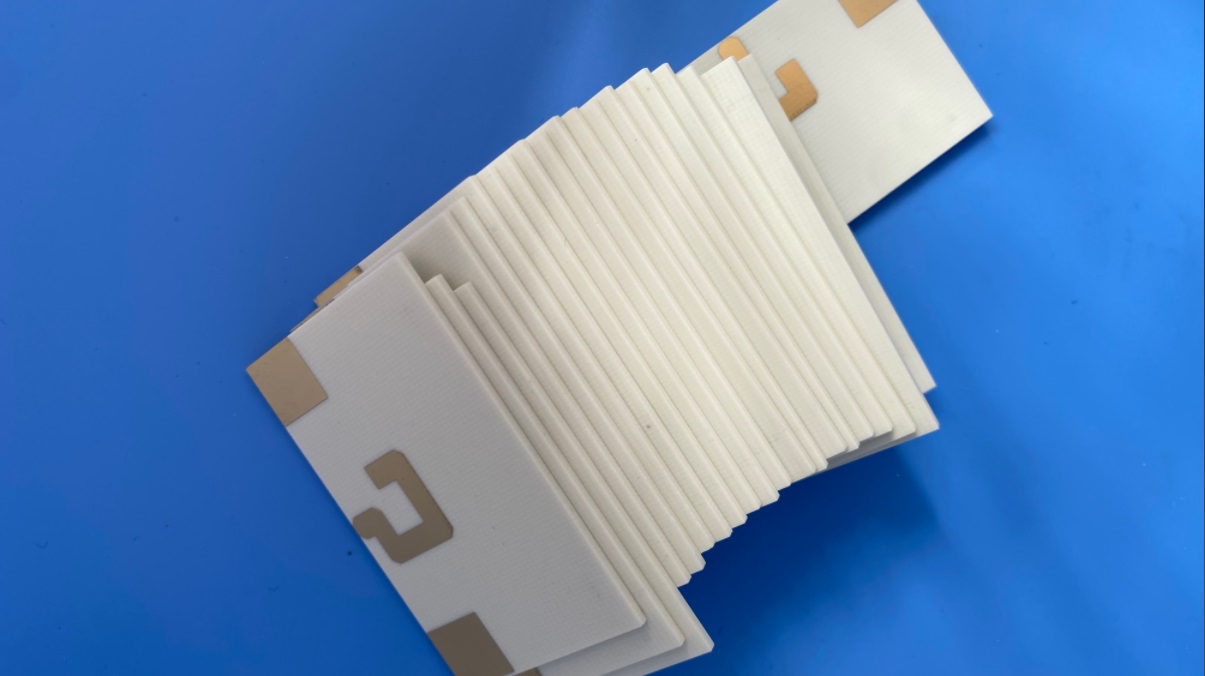
In the demanding landscape of high-frequency electronics, Rogers 5870 laminates stand as a pinnacle of engineering excellence. These PTFE-based composites, reinforced with randomly dispersed glass microfibers, deliver unparalleled dielectric consistency—making them the substrate of choice for precision stripline and microstrip circuitry. Engineered to thrive in broadband and high-frequency environments, RT/duroid 5870 Material minimizes signal dispersion and energy loss while extending operational efficiency into the Ku-band and beyond.


Critical Performance Attributes

1.Ultra-Low Dielectric Properties

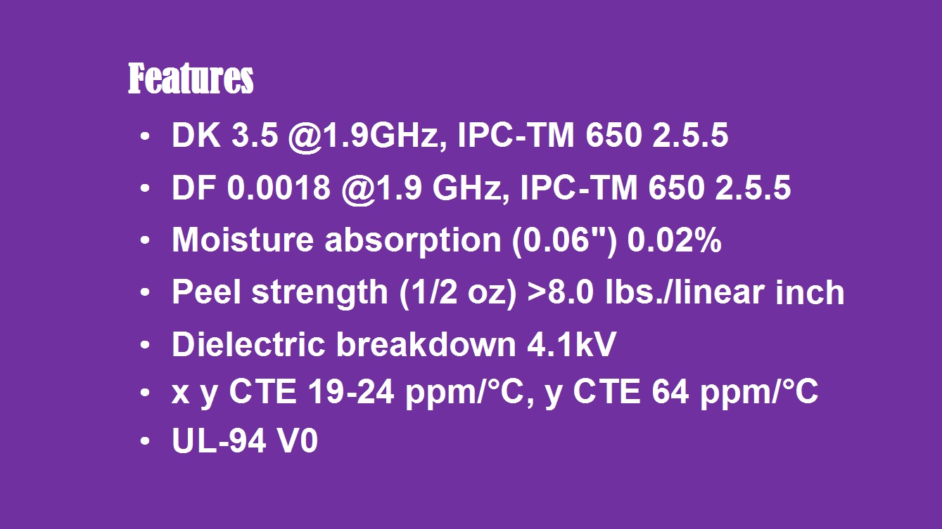
With a dielectric constant (Dk) of 2.33 and dissipation factor (Df) of 0.0012 (verified at 10 GHz),Duroid 5870 PCBensures minimal signal delay and attenuation. These properties enable high-speed signal integrity for 5G infrastructure, satellite communications, and phased-array radar.


2.Moisture Resistance for Harsh Environments

Leveraging inherent PTFE characteristics, the material exhibits remarkably low moisture absorption (0.02%). This resilience guarantees stable performance in high-humidity conditions—critical for avionics, maritime systems, and tropical deployments.


3.Unmatched Signal Integrity

As the lowest-loss reinforced PTFE material available,Rogers RT/Duroid 5870 provides isotropic behavior with uniform electrical properties across all axes. This eliminates directional performance variances, ensuring consistent impedance control for multi-layer RF designs.


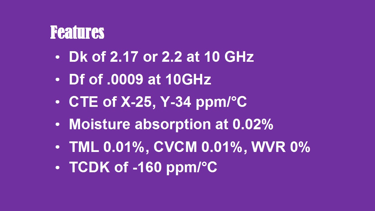
RT duroid 5870 pcb features


Advanced PCB Manufacturing Capabilities

We deliver end-to-end solutions for Duroid 5870 High Frequency PCB-based circuits, supporting the most complex high-frequency applications:


Structural Versatility

Layer Configurations: Single-layer, double-layer, multi-layer (up to 24 layers), and hybrid stacks combining FR-4/Rogers materials.

Thickness Range: Standard options from 10 mil to 62 mil, including 15 mil, 20 mil, and 31 mil profiles. Custom thicknesses available.

Panel Scalability: Maximum panel size of 400mm×500mm—ideal for large-format antennas or multi-project arrays.


Surface Engineering

Copper Weights: 1oz or 2oz finished copper with±0.07 mil tolerance. 

Solder Masks: Green, black, blue, red, yellow, and matte finishes.

Surface Finishes:

Immersion Gold (ENIG)

HASL (Lead/Lead-free)

Immersion Silver/Tin

ENEPIG (for wire bonding)

Electrolytic Hard Gold

OSP & Bare Copper


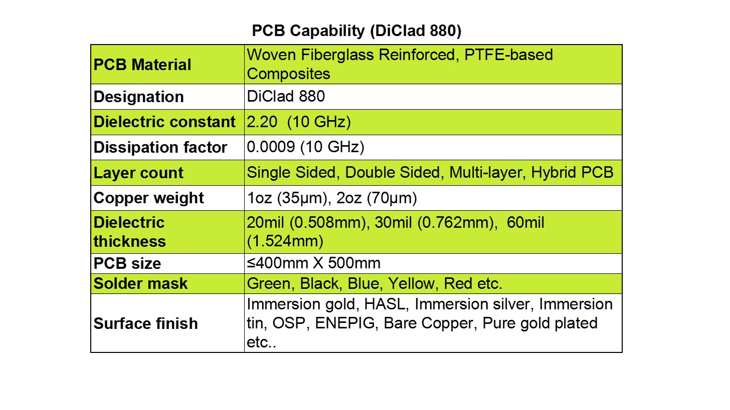
Rogers 5870 PCB Capability


Mission-Critical Applications

Rogers 5870’s blend of electrical stability and environmental endurance makes it indispensable across defense, aerospace, and telecom sectors:


  • Aerospace: Airborne broadband antennas, collision avoidance systems.
  • Military: Radar arrays, missile guidance PCBs, electronic warfare modules.
  • Telecom: Point-to-point radio antennas, millimeter-wave backhaul links.
  • Emerging Tech: Automotive radar (77/79 GHz), quantum computing interconnects.


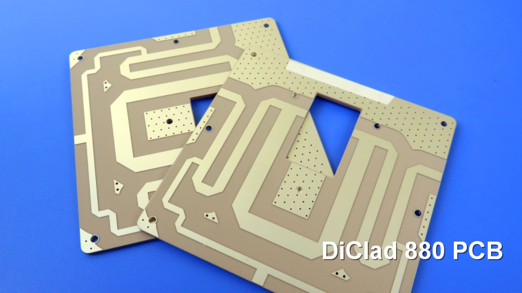
 RT/duroid 5870 high frequency PCBs


Why Partner with Us?

As an ISO 9001-certified supplier, we combine Rogers material expertise with:


  • Impedance Control:±5% tolerance via TDR testing.
  • Hybrid Bonding: Seamless integration of RT/duroid 5870 with FR-4/ceramics.
  • High-Tg Processing: Lamination cycles optimized for PTFE’s low thermal expansion.
  • DFM Support: Signal layer adjacency planning and via optimization.


Industry Challenge Solved: Traditional FR-4 laminates suffer from erratic Dk values above 6 GHz. RT/duroid 5870’s glass microfiber matrix eliminates this variability—enabling precise phase matching in 40 GHz beamforming networks.


Conclusion

For engineers pushing the boundaries of high-frequency design,RT/duroid 5870 high frequency PCBs deliver uncompromised signal fidelity, thermal resilience, and manufacturing flexibility. Whether developing next-gen radar or satellite payloads, this material system bridges the gap between theoretical performance and real-world reliability.

What Makes RT/duroid 6002 the Premier Choice for Demanding High-Frequency PCB Applications?


In the relentless pursuit of performance within the RF and microwave sector, the selection of printed circuit board (PCB) substrate material is a critical determinant of success. For engineers designing cutting-edge systems where signal integrity, thermal management, and reliability are non-negotiable, Rogers Corporation's RT/duroid 6002 laminates emerge as a superior microwave material solution. This advanced composite, engineered with ceramic-filled polytetrafluoroethylene (PTFE), is specifically formulated to meet the rigorous demands of complex microwave structures, offering an unparalleled blend of electrical and mechanical properties that guarantee exceptional performance and longevity in multi-layer board constructions.


Exceptional Material Properties for Peak Performance

The standout characteristics of Rogers 6002 laminates are rooted in their precise and stable electrical properties, which are meticulously tailored for high-frequency applications.


Rogers 6002 features


1.Consistent Dielectric Constant:

With a dielectric constant (Dk) of 2.94 and an exceptionally tight tolerance of±0.04, these laminates provide a stable electrical environment that is paramount for impedance control. This consistency is vital for maintaining signal integrity, minimizing reflection, and ensuring predictable performance across the entire board.


2.Superior Thermal Stability:

A common challenge in high-frequency applications is performance drift caused by temperature fluctuations. The Rogers RT/duroid 6002 addresses this with an ultra-low thermal coefficient of dielectric constant (12 ppm/°C). This ensures that the Dk value remains stable over a broad temperature range, safeguarding the electrical performance of your design against thermal variations and ensuring operational consistency in diverse environments.


3.Minimal Signal Loss:

The dissipation factor (loss tangent) is a crucial metric for efficiency. At a remarkably low value of 0.0012 at 10 GHz, RT/duroid 6002 exhibits minimal electrical energy loss, converting it into heat. This translates to highly efficient transmission of microwave signals, reduced attenuation, and enhanced overall signal quality, which is essential for long-range and sensitive communication systems.


4.Enhanced Mechanical Reliability:

Beyond electrical performance, the laminate’s low Z-axis coefficient of thermal expansion (CTE) of 24 ppm/°C is a key feature for structural integrity. This characteristic signifies outstanding dimensional stability, drastically reducing the risk of warping, delamination, or plated through-hole failure when the board is subjected to thermal cycling during assembly and operation. This inherent stability is a cornerstone for building reliable, high-layer-count multilayer boards.


Advanced PCB Manufacturing Capabilities for RT/duroid 6002

Leveraging the superb properties of this material requires a manufacturing partner with precise expertise. Our specialized PCB fabrication services are optimized to fully harness the potential ofRogers RT/duroid 6002 material, offering extensive flexibility to meet your exact design requirements.


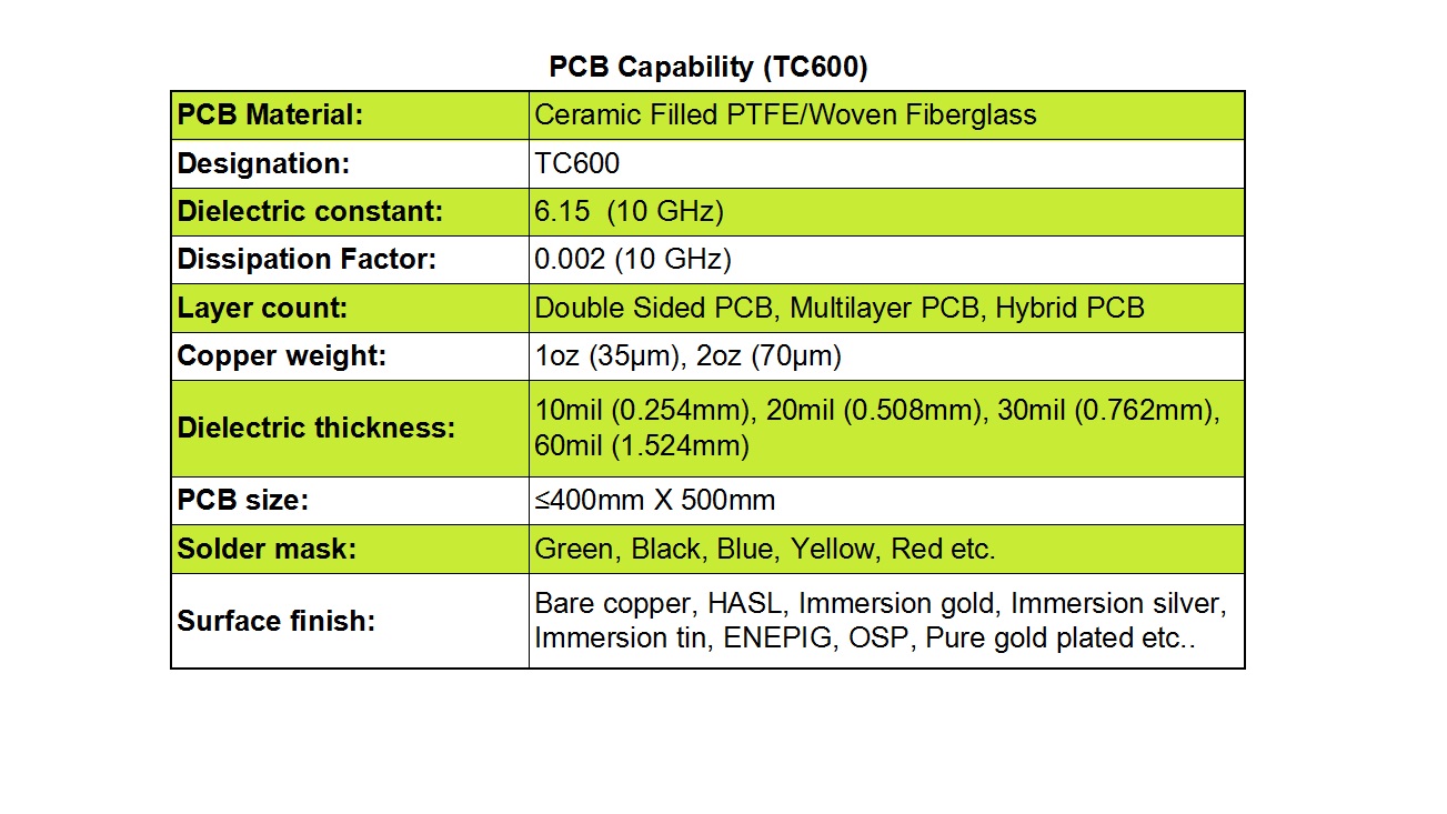
RT/duroid 6002 PCB Manufacturing Capabilities


1.Layer Configuration Versatility:

We support a comprehensive range of structures, from simple 1-layer and 2-layer boards to sophisticated multi-layer and hybrid designs that incorporate other materials for optimized cost and performance.


2.Customizable Construction: 

To achieve target impedances and manage current loads, we accommodate standard copper weights of 1oz (35µm) and 2oz (70µm). Furthermore, we provide a selection of precise PCB thicknesses, including 10mil (0.254mm), 20mil (0.508mm), 30mil (0.762mm), 60mil (1.524mm), and 120mil (3.048mm).


3.Larger Format Boards: 

Our production capabilities can accommodate PCB sizes up to 400mm x 500mm, providing ample real estate for larger, more complex circuitry often found in advanced radar and antenna systems.


4.Finishing Options:

We offer a variety of solder mask colors (Green, Black, Blue, Yellow, Red, etc.) and a complete suite of surface finishes. These include Bare Copper, HASL, ENIG, Immersion Silver, Immersion Tin, pure Gold (directly on copper), ENEPIG, and OSP, ensuring optimal solderability and protection for your specific application.


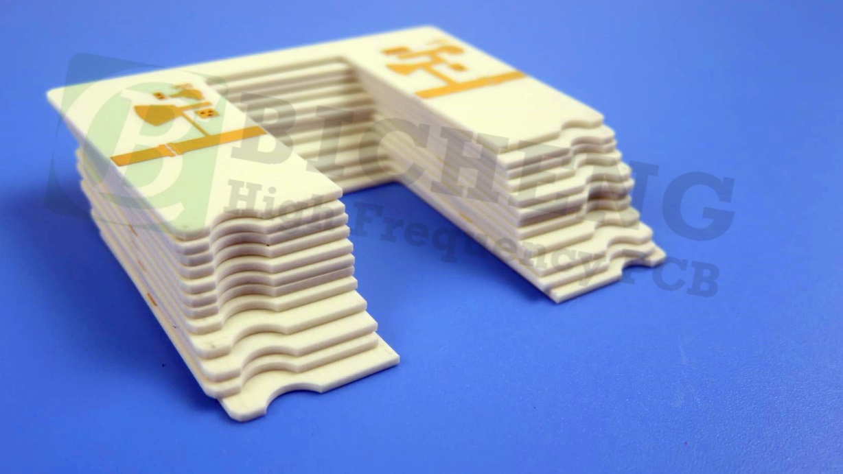
RT/duroid 6002 High Frequency PCBs


Broad-Ranging Applications

The unique combination of electrical and mechanical properties makes RT/duroid 6002 High Frequency PCBs the material of choice for a wide array of critical, high-performance applications. These include:


-Phased Array Antennas

-Ground-Based and Airborne Radar Systems

-Global Positioning System (GPS) Antennas

-High-Speed Power Backplanes

-Commercial Airline Collision Avoidance Systems


Conclusion

For designers pushing the boundaries of RF and microwave technology, the substrate is not just a foundation—it's an active component of the system's performance. Rogers RT/duroid 6002 substrates, with their proven low-loss, stable Dk, and outstanding reliability, provide the technical excellence required for next-generation applications. Partner with a supplier that possesses the advanced manufacturing capabilities to transform this exceptional material into a high-precision, reliable PCB that will elevate your product's performance. Contact us today to discuss your project requirements and discover how our expertise can benefit your next high-frequency design.


Why Choose RO3003 High Frequency PCBs for Stable RF/Microwave Performance?


Introduction

RO3003 high-frequency laminates represent a breakthrough in advanced circuit materials, engineered to deliver unparalleled electrical performance, mechanical resilience, and economic efficiency. As a ceramic-reinforced PTFE (polytetrafluoroethylene) composite, these laminates provide a superior solution for demanding microwave and RF applications. Their ability to maintain consistent signal integrity across extreme frequencies positions Rogers RO3003 as an indispensable material for next-generation technologies.


In environments where thermal and frequency fluctuations challenge conventional materials, Rogers RO3003 PCB excels with its remarkably stable dielectric constant. This stability is critical for automotive radar systems operating at 77 GHz, millimeter-wave 5G infrastructure, and Advanced Driver Assistance Systems (ADAS), where precision signal propagation directly impacts safety and functionality. By minimizing phase shifts and impedance variations, Rogers 3003 laminates ensure reliable performance in mission-critical applications.


Electrical & Mechanical Properties


ro3003 features


2.1 Precision Dielectric Characteristics


  • Dk Stability: With a dielectric constant (Dk) of 3.00±0.04 across temperature and frequency ranges, RO3003 enables predictable impedance control essential for high-frequency designs.


  • Ultra-Low Signal Loss: A dissipation factor of 0.0010 at 10 GHz minimizes insertion loss, preserving signal strength in mmWave applications up to 77 GHz and beyond.


2.2 Thermal Reliability


  • Minimal CTE Variation: CTE values of 17 ppm/°C (X-axis), 16 ppm/°C (Y-axis), and 25 ppm/°C (Z-axis) prevent delamination and via cracking during thermal cycling.
  • Thermal Consistency: Maintains electrical properties from -50°C to +150°C, ideal for automotive underhood electronics and outdoor RF infrastructure.


2.3 Quality & Cost Efficiency


  • ISO 9001-Certified Manufacturing: Guarantees batch-to-batch consistency and compliance with international quality standards.
  • Budget Optimization: Delivers RF performance comparable to premium laminates at 30–40% lower cost, reducing BOM expenses without sacrificing reliability.


 RO3003 BENEFITS


Advanced PCB Manufacturing Capabilities for RO3003

To fully leverage RO3003 High Frequency PCB’s properties, our manufacturing processes ensure precision and flexibility:


RO3003 Manufacturing Capabilities


Layer Count Versatility:

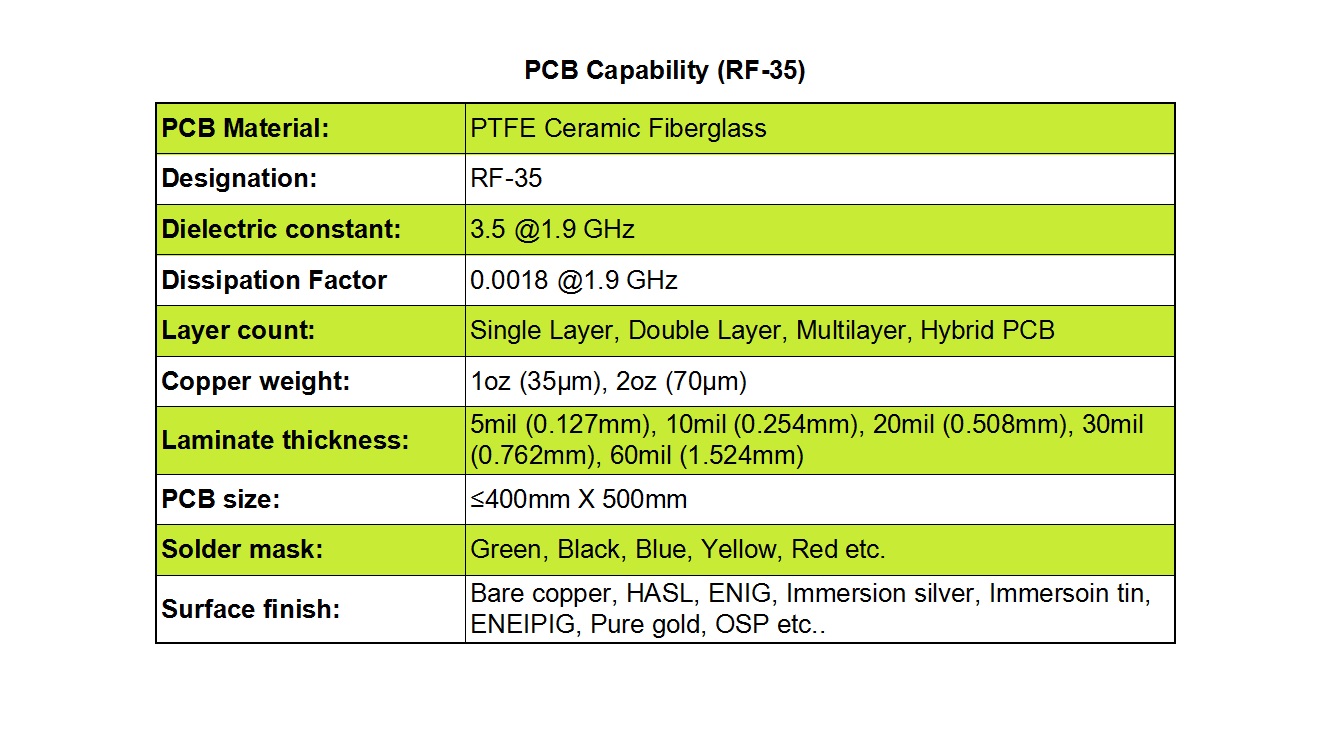
We accommodate diverse design complexities, expertly manufacturing Single Sided, Double Sided, Multi-layer PCBs (including complex HDI designs), and Hybrid constructions combining RO3003 with other specialized materials for optimal performance and cost management.


Flexible Copper Weights: 

Tailor current carrying capacity and trace characteristics with standard options like 1oz (35µm) and 2oz (70µm) copper foil, with custom weights available to meet specific RF and thermal requirements.


Precise Dielectric Thickness Control:

Achieve the exact impedance and performance targets with a wide range of dielectric thicknesses, spanning from a thin 5mil (0.127mm) up to a robust 60mil (1.524mm).


Generous Panel Sizing:

Our production capacity supports PCB panels up to 400mm x 500mm, efficiently handling larger boards or optimizing panelization for smaller components.


Solder Mask Options: 

Maintain brand identity or functional needs with a selection of solder mask colors, including Green, Black, Blue, Yellow, Red, and others.


Comprehensive Surface Finishes: 

Ensure optimal solderability, wire bonding capability, shelf life, and signal integrity by choosing from our full range of surface finishes:


  • Immersion Gold (ENIG)
  • Hot Air Solder Leveling (HASL - Leaded or Lead-Free)
  • Immersion Silver
  • Immersion Tin
  • Electroless Nickel Electroless Palladium Immersion Gold (ENEPIG)
  • Organic Solderability Preservative (OSP)
  • Bare Copper (for specific controlled environments)
  • Pure Gold (Hard Gold) for edge connectors or demanding wear applications.


 Rogers 3003 pcb


Critical Applications Leveraging RO3003

1. Automotive Radar Systems:

77 GHz long-range radar (LRR) and short-range radar (SRR) sensors for adaptive cruise control and collision avoidance.

Low moisture absorption (<0.1%) ensures performance in humid environments.


2. 5G Infrastructure:

mmWave base station antennas (24–43 GHz) requiring stable Dk across temperature gradients.

Massive MIMO arrays with ultra-low loss feed networks.


3. Aerospace & Telecommunications:

GPS/GNSS satellite antennas with precise phase stability.

5G NR small cells and remote meter readers operating in harsh outdoor conditions.


4. High-Power RF Systems:

Power backplanes and military-grade radar utilizing Z-axis CTE stability for plated-through-hole reliability.


Conclusion

RO3003 high frequency PCBs bridge the gap between cutting-edge electrical performance and manufacturability. With industry-leading Dk stability, minimal loss characteristics, and rigorous quality certification, this laminate empowers designers to push the boundaries of 77 GHz automotive radar, 5G mmWave, and ADAS innovations. Partner with us to access full-spectrum manufacturing capabilities—from rapid prototyping to complex hybrid stacks—tailored to your application’s unique demands.


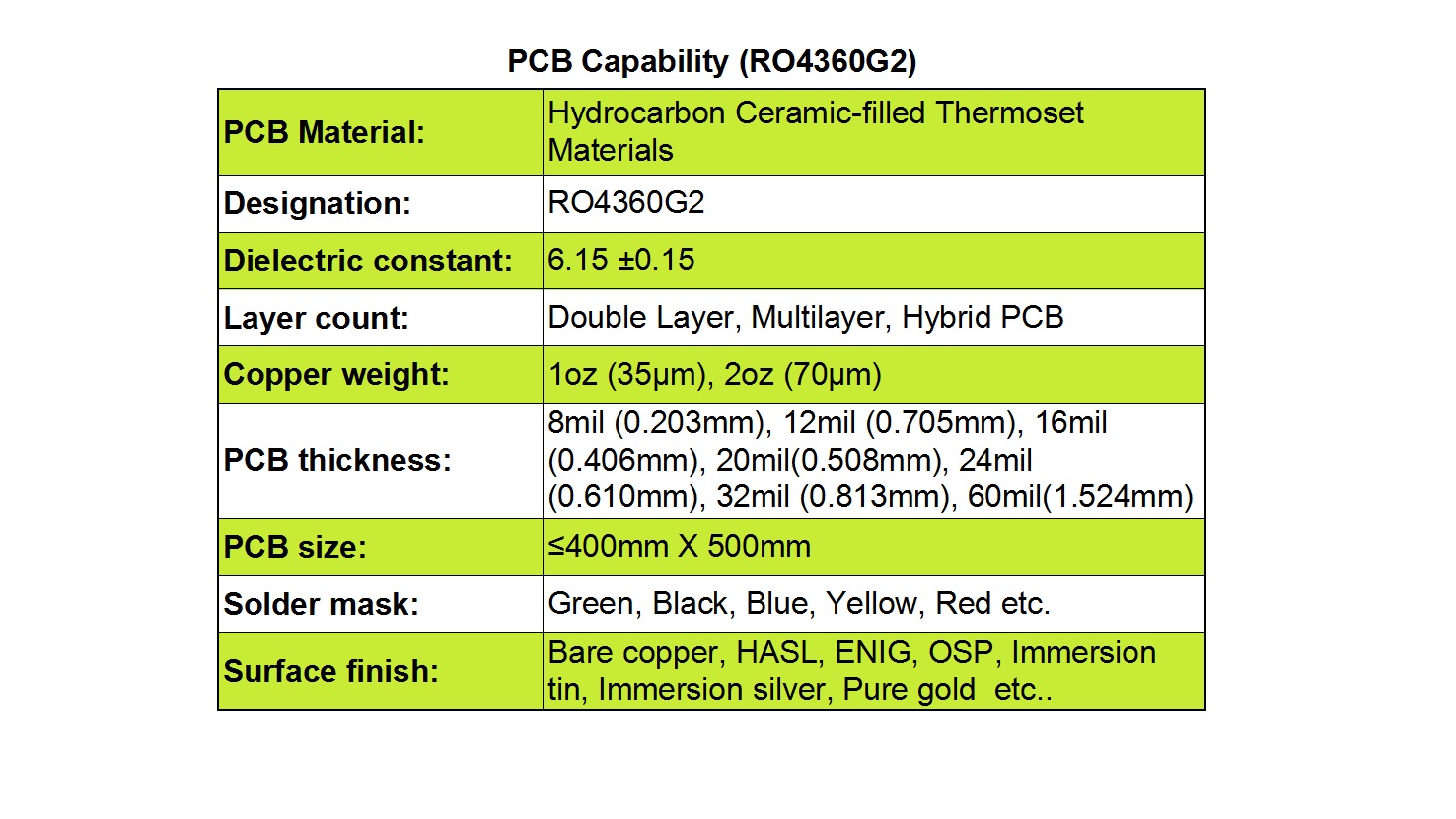
Why Choose RO4003C High Frequency PCBs for Superior RF Performance & Cost Efficiency?


Introduction

Rogers RO4003C high-frequency laminates revolutionize RF/microwave design by merging exceptional electrical properties with streamlined manufacturability. Engineered with proprietary hydrocarbon/ceramic matrices reinforced with precision-woven glass, these substrates deliver PTFE-level signal integrity while adopting the fabrication processes of conventional epoxy/glass composites. Available in both 1080 and 1674 glass fabric configurations, RO4003C guarantees uniform dielectric behavior across diverse layouts. Critically, it maintains ultra-tight dielectric constant (Dk) tolerances and minimizes insertion losses without requiring specialized processing infrastructure. This unique combination slashes production costs by up to 40% compared to legacy microwave laminates while sustaining uncompromised high-frequency performance–making it the pragmatic choice for next-generation RF systems.


Core Features & Performance Advantages


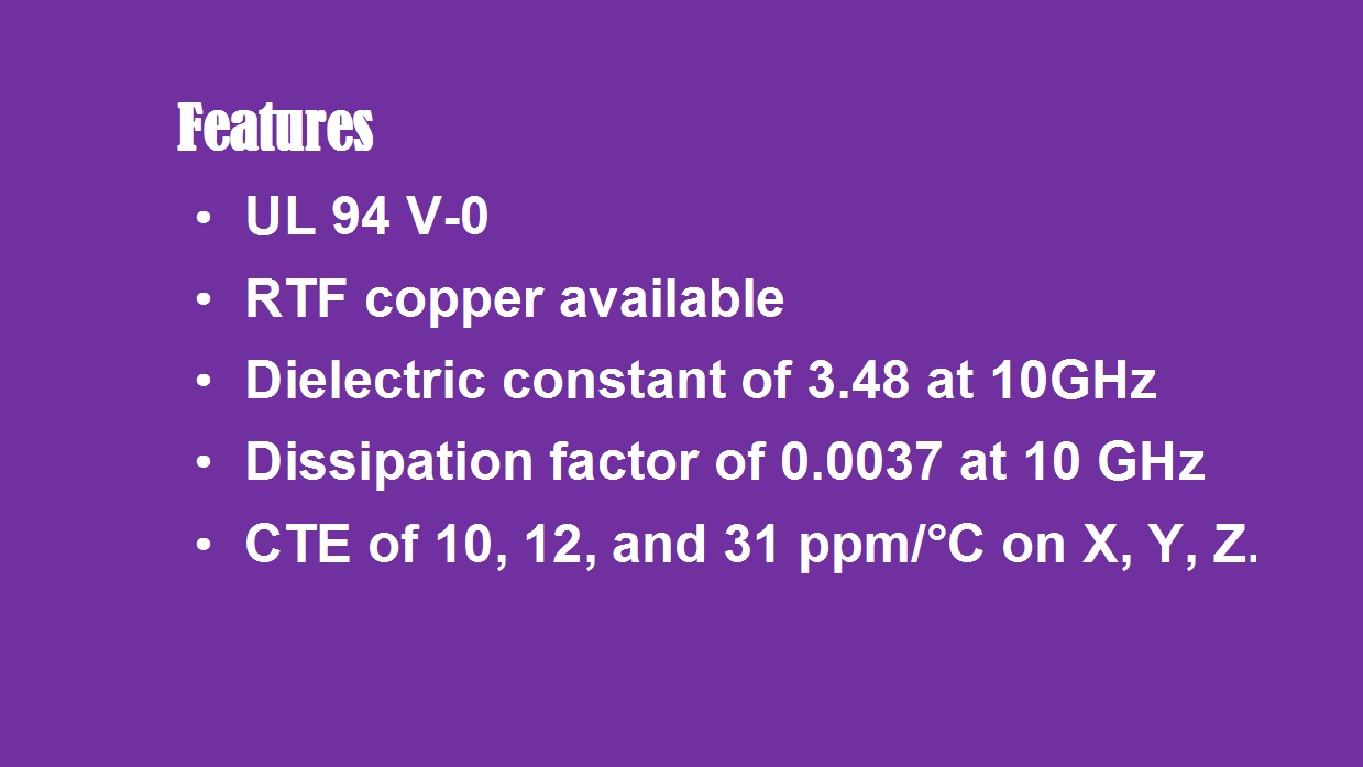
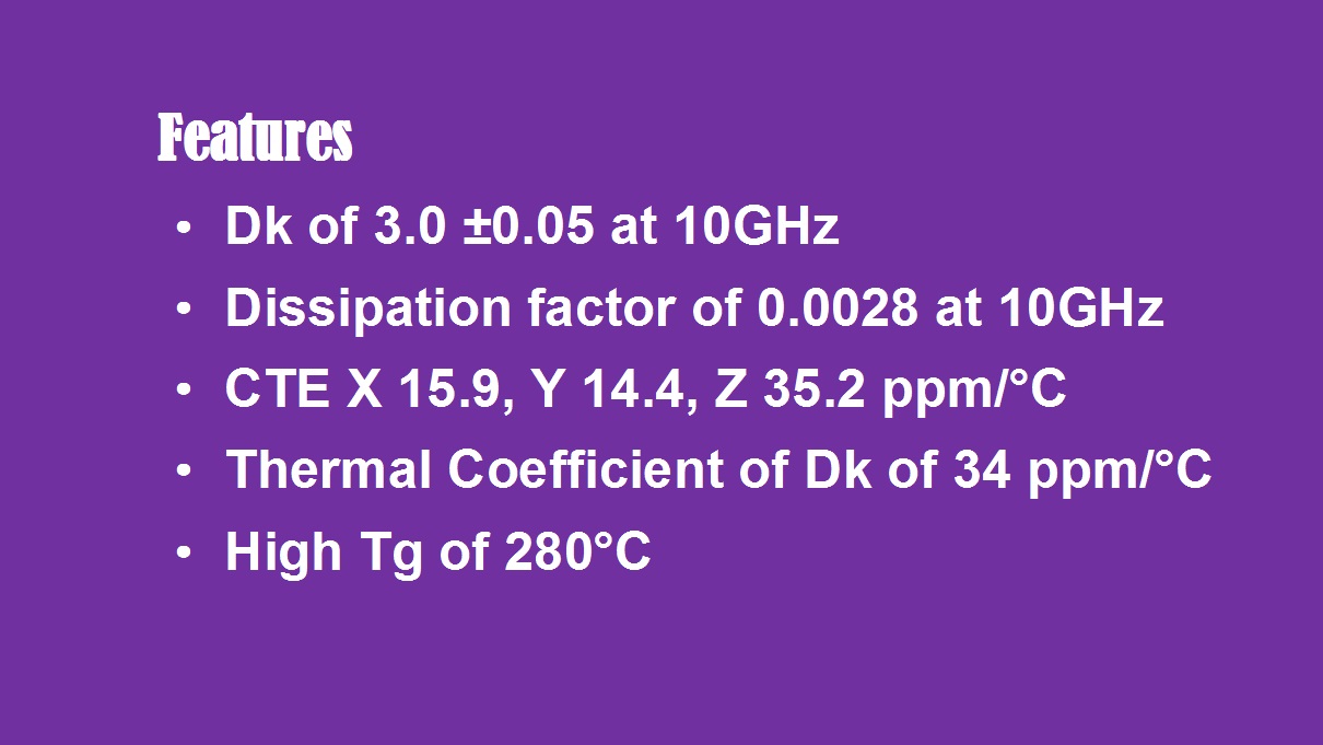
RO4003C feature


1. Dielectric Constant Stability:

RO4003C’s hallmark Dk value of 3.38 (±0.05) provides unmatched stability across temperature fluctuations and frequency bands. This consistency enables precise impedance matching (critical for 50Ω/75Ωsystems) and eliminates phase distortion in multi-channel arrays like beamforming antennas.


2. Ultra-Low Dissipation & Signal Loss:

With a remarkably low dissipation factor (Df) of 0.0027 at 10 GHz, Rogers 4003C minimizes dielectric absorption losses. This translates to higher Q factors in resonators, extended range in RFID tags, and enhanced efficiency in 5G power amplifiers operating at mmWave frequencies.


3. Thermal Reliability for Demanding Environments:

Featuring a Z-axis CTE of just 46 ppm/°C–closely matching copper’s expansion rate–RO4003C prevents plated through-hole (PTH) barrel cracking during thermal cycling. This robustness supports automotive radar modules (-40°C to +150°C operational ranges) and aerospace systems encountering extreme thermal shocks.


4. FR-4 Process Compatibility:

Unlike costly PTFE-based alternatives, RO4003C substrate leverage existing FR-4 manufacturing workflows. This compatibility slashes fabrication costs by eliminating specialized equipment or processes, making high-frequency performance economically accessible for multilayer boards (MLBs).


Advanced PCB Manufacturing Capabilities


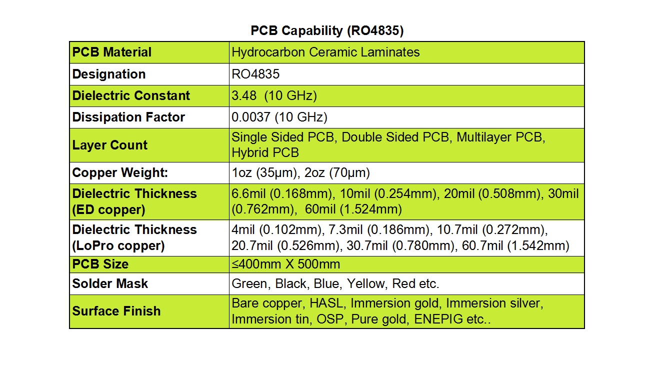
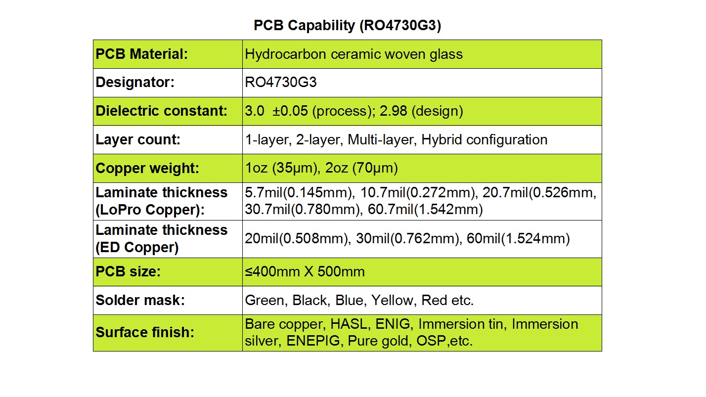
RO4003C PCB CAPABILITY


Layer Flexibility & Construction

We support diverse design complexities through:


  • Layer Options: Double-sided, multilayer (up to 32 layers), and hybrid stacks.
  • Copper Weights: 1oz (35µm) and 2oz (70µm) for optimized current handling and thermal management.


Material Thickness

Select from RO4003C core thicknesses tailored to your electrical and mechanical needs:


  •  Standard Thicknesses: 8mil (0.203mm), 12mil (0.305mm), 16mil (0.406mm), 20mil (0.508mm), 32mil (0.813mm), and 60mil (1.524mm).


Critical Fabrication Specifications:


  • Max Panel Size: 400mm×500mm (supports arrayed LNBs and large-format antenna panels)


Solder Mask: 


  • Green (standard), Black/Blue (high-contrast alignment), or custom colors (Red/Yellow for test vehicles)


 Surface Finishes:


  • HASL: Cost-effective consumer RFIDs
  • ENIG/ENEPIG: Gold wire-bondable PA modules
  • Immersion Ag/Sn: Lead-free automotive sensors
  • Flash Gold: High-reliability satellite comms


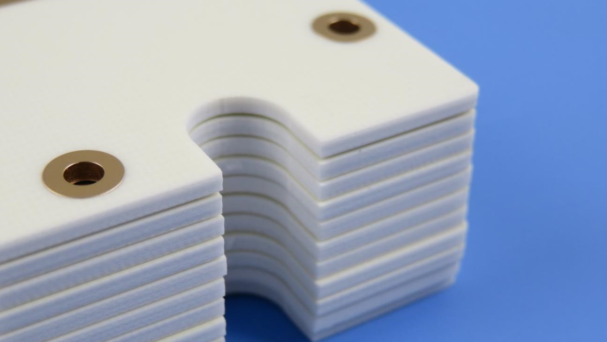
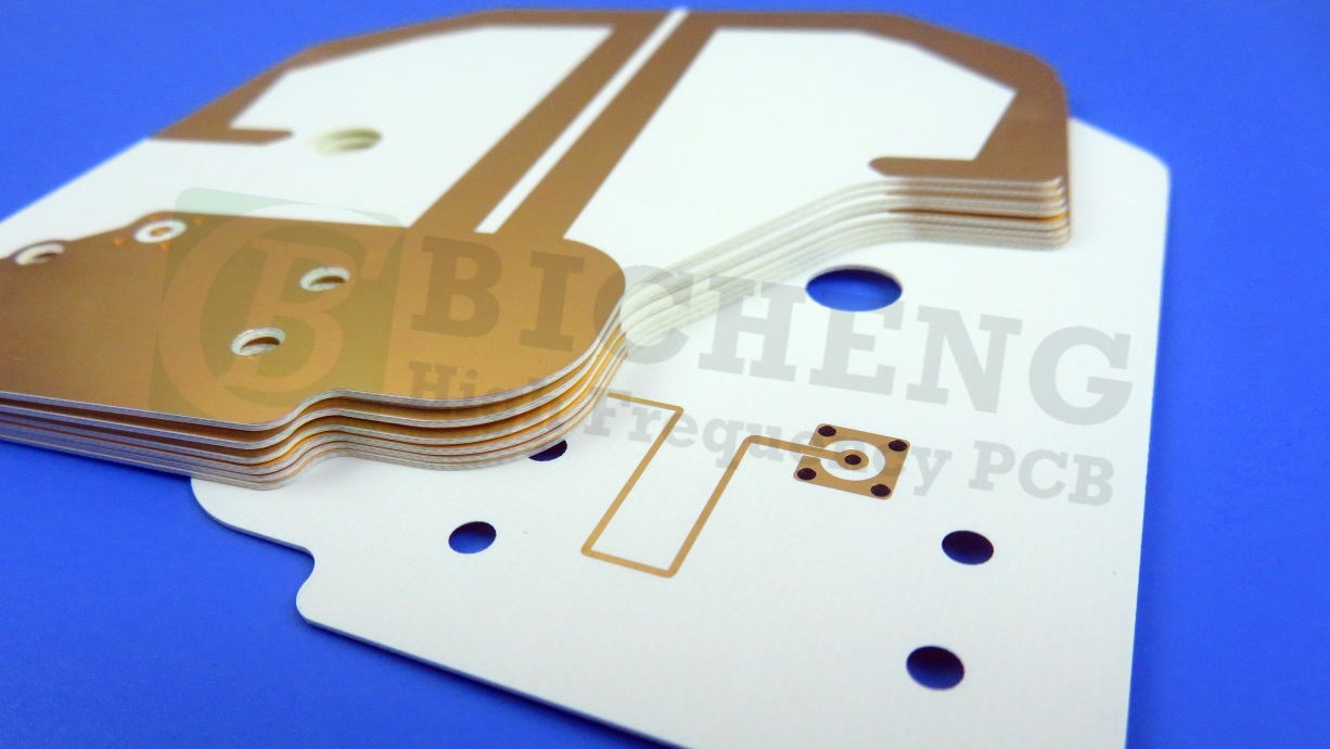
 Rogers 4003C PCB


Industry-Leading Applications

Rogers RO4003C PCB excel in high-frequency environments demanding precision and durability: 


  • Telecom: 5G base station antennas, power amplifiers.
  • Automotive: Radar sensors (77 GHz), ADAS modules.
  • Aerospace: Satellite LNBs (Low-Noise Block downconverters).
  • IoT: RFID tags, industrial sensors.


Why Partner with Us?

As a certified PCB supplier, we combine cutting-edge RO4003C materials with:


  • Hybrid PCB Expertise: Seamlessly integrate FR-4 and RO4003C layers.
  • Rigorous Testing: Ensure signal integrity via TDR and impedance control.
  • Rapid Prototyping: Accelerate development cycles without sacrificing quality.


Conclusion: The Cost-Performance Breakthrough

Rogers RO4003C High Frequency PCB resolve the traditional dilemma between electrical performance and manufacturability. By delivering PTFE-grade signal integrity via FR-4 production flows, they accelerate time-to-market for 5G, radar, and satellite systems while reducing total board costs by 25–40%. With our extensive processing capabilities–spanning hybrid designs, advanced finishes, and large-format panels–your high-frequency projects gain both technical superiority and supply-chain agility.

Why Should You Choose TMM4 Thermoplastic Microwave Material for Your Next RF and Microwave Project?


In the world of high-frequency electronics, the choice of printed circuit board (PCB) material is critical to the performance, reliability, and overall success of an application.Rogers TMM4 stands out as an exceptional thermoset microwave composite material specifically engineered to provide outstanding plated-through-hole reliability. It is ideally suited for a variety of high-frequency designs, including sophisticated strip-line and micro-strip circuit configurations. By uniquely combining the beneficial properties of ceramic fillers, hydrocarbon resins, and thermoset polymers,TMM4 delivers a superior blend of electrical, mechanical, and thermal characteristics. This makes it a highly robust and dependable substrate that meets the stringent demands of advanced microwave and RF systems.


A significant advantage of TMM4 laminates is their ability to provide the high performance of ceramic and traditional PTFE-based materials without the associated manufacturing complexities. These laminates are based on a user-friendly thermoset resin system, which streamlines the Rogers PCB fabrication process. This inherent ease of processing eliminates the need for specialized equipment or techniques often required for polytetrafluoroethylene (PTFE) materials. Furthermore, the robust thermoset structure guarantees excellent wire-bonding integrity, virtually eliminating concerns such as pad lifting or substrate deformation during assembly or operation.


Key Features and Performance Advantages

The exceptional performance of TMM4 High-Frequency PCBs is anchored in a set of well-defined and stable material properties:


TMM4 Features


1.Stable Dielectric Properties: 

TMM4 exhibits a consistent dielectric constant (Dk) of 4.50 with a very tight tolerance of±0.045. This stability is paramount for maintaining impedance control and signal integrity across the board. Coupled with an ultra-low dissipation factor (loss tangent) of 0.0020 at 10 GHz, TMM4 ensures minimal signal loss, enabling efficient and clean signal transmission even in high-power and high-frequency scenarios.


2.Excellent Thermal Stability:

The electrical performance of TMM4 remains highly consistent across a wide temperature range, thanks to its remarkably low thermal coefficient of dielectric constant (20 ppm/°C). This means the material's Dk does not drift significantly with temperature fluctuations, which is crucial for applications exposed to varying environmental conditions. Its thermal expansion properties are meticulously matched to copper, with CTE values of 16 ppm/°K in the X and Y axes and 21 ppm/°K in the Z-axis. This CTE matching significantly reduces mechanical stress on plated through-holes during thermal cycling, dramatically enhancing the long-term reliability and longevity of the PCB.


3.Superior Thermal Performance:

TMM4 substrates are built to withstand harsh operating environments. They possess a high decomposition temperature (Td) of 425°C as measured by TGA, ensuring material integrity during high-temperature soldering processes and in end-use applications. A thermal conductivity of 0.7 W/m/K allows for effective heat dissipation away from active components, which is vital for maintaining performance and preventing overheating in power amplifiers and other heat-generating circuits.


4.Low Moisture Absorption:

The hygroscopic nature of a PCB substrate can severely impair its electrical properties. TMM4 demonstrates outstanding resistance to moisture, with absorption rates as low as 0.07% for a 50mil thickness and 0.18% for a 125mil thickness. This low moisture uptake ensures stable electrical performance and prevents delamination or other moisture-induced failures, even in humid conditions.


Advanced PCB Manufacturing Capabilities with TMM4

Our state-of-the-art manufacturing facilities are fully equipped to handle TMM4 laminates, transforming their inherent material advantages into high-performance, reliable PCBs. We offer comprehensive solutions tailored to your specific design requirements.


TMM4 PCB Capability


1.PCB Type: 


  • Single-sided, Double-sided, Multi-layer, and Hybrid Constructions (combining TMM4 with other materials) 


2.Copper Weight 


  • (Finished):1 oz (35 µm) and 2 oz (70 µm)


3.Laminate Thickness:


  • From 15mil (0.381mm) and 25mil (0.635mm) up to 500mil (12.7mm), including 30mil, 50mil, 60mil, and more.


4.Max. Panel Size:


  • Up to 400mm x 500mm


5.Solder Mask Colors:


  • Green, Black, Blue, Yellow, Red, and more


6. Surface Finish Options:


  • Bare Copper, HASL, ENIG, Immersion Tin, Immersion Silver, Pure Gold (no nickel), OSP, ENEPIG, and others.


This extensive range of capabilities provides design engineers with the flexibility needed to push the boundaries of their high-frequency designs without being constrained by manufacturing limitations.


Typical Applications

The unique property set of TMM4 high frequency PCB makes it the material of choice for a wide spectrum of demanding high-frequency electronic applications, including:


TMM4 high frequency PCB


1.Telecommunications Infrastructure: 

Power amplifiers, combiners, filters, and couplers for base stations and network equipment.


2.Aerospace and Satellite Systems:

Satellite communication transceivers, GPS antenna systems, and onboard radar systems where reliability is non-negotiable.


3.Radar and Sensing Systems:

Patch antennas and array antennas for automotive radar, industrial sensing, and defense applications.


4.Test and Measurement:

High-performance chip testers, probe cards, and RF test fixtures that require stable and low-loss signal paths.


Conclusion

For engineers and designers tasked with developing next high-frequency circuits, Rogers TMM4 presents a compelling solution. It successfully bridges the gap between the high performance of ceramic and PTFE laminates and the manufacturability and reliability of thermoset resins. By choosing TMM4 and partnering with a capable PCB supplier, you can achieve superior electrical performance, enhanced thermal management, and unwavering reliability in your most critical applications. Contact us today to discuss how we can leverage TMM4 laminates to optimize your next high-frequency PCB project.

With the rapid development of the new energy vehicle market, as a core component for energy transmission, the cost control and optimization of high-voltage wiring harnesses have become the key for automakers to enhance their competitiveness. Wire harness experts conduct an analysis from three dimensions: cost structure, quotation process, and cost reduction strategies. By integrating industry practice and technological innovation, they systematically expound the full life cycle management methods for EV high-voltage wire harnesses.


I. In-depth Analysis of High-Voltage Wiring Harness Costs

(1) Cost composition model

The total cost of HV wiring harnesses consists of material costs (73.8%), processing fees (14.7%), packaging and transportation fees (2%), and management fees (9.5%). Among them, the proportion of material costs is the highest, specifically including:

1. High-voltage connectors (55%) : They are responsible for electrical connection and signal transmission. The price difference between foreign brands (such as TE) and domestic brands (such as Luxshare) can reach 30%.

2. High-voltage cables (35%) : Copper conductor materials are dominant, with a cross-sectional area range of 16-150mm². The cost increases exponentially with the increase in wire diameter. Take a 50mm² cable as an example, the cost per meter is approximately 50 to 80 yuan.

3. Coating materials (6%) : including corrugated tubes, heat shrink tubes, etc., with a temperature resistance grade of over 150℃. Although the cost proportion is low, it affects the protective performance.

4. Other auxiliary materials (4%) : Shielding layer (aluminum foil + braided copper mesh), guard plate, etc. The material selection directly affects the EMC performance.


(II) Cost-sensitive factors

1. Wiring harness length: After the fast charging wiring harness length of a certain model was optimized from 4 meters to 2.5 meters, the cost decreased by 260 yuan.

2. Number of connectors: The high-voltage system architecture has been optimized to reduce 4 connectors, which can save 730 yuan in costs.

3. Process complexity: Replacing the crimping process with ultrasonic welding can increase efficiency by 15%, but the equipment investment increases by 20%.


Ii. Quotation Process and Key Control Points for High-Voltage Wiring Harnesses

(1) Standardized quotation process

In the requirements confirmation stage, obtain the vehicle's electrical schematic diagram, 3D wiring diagram and technical parameters (voltage level, current load, etc.).

2. Clearly define core indicators such as protection level (IP67/IP6K9K) and EMC shielding effectiveness (≥85%).

3. Use CATIA for 3D wiring simulation to avoid mechanical interference and optimize the path, reducing the length of the wiring harness by 10% to 15%.


4. Select the connector model (such as HVP800 series) and cable specification to form a BOM list.

5. Cost accounting Model:

5.1 Material cost: Calculated based on the unit price of cables (such as 70 yuan per meter for 50mm² copper cables) and the unit price of connectors (approximately 150 yuan per set for domestic products).

5.2 Processing fees: Priced by process, including crimping (0.5 yuan per point), shielding treatment (1.2 yuan per meter), etc.

5.3 Additional charges: Packaging and transportation (3-5 yuan per set), testing and certification (for example, QC/T 1037 testing fee is approximately 5,000 yuan per batch).

6. Comprehensive quotation output

6.1 Provide itemized quotations and reserve a margin of 5% to 10% for engineering changes.

(II) Key Links in Cost Control

1. Design collaboration: Conduct joint reviews with the original equipment manufacturer to avoid redundant functional designs (such as combining HVH and PTC functions to save 1.5m of wiring harnesses).

2. Supplier Management: Establish a certification system for domestic connectors (such as Ebusbar) to replace TE, reducing procurement costs by 25%.

3. Process validation: Through DOE tests, the crimping parameters (pressure of 3-5 tons, holding time of 0.5 seconds) were optimized, increasing the yield to 99.5%.


Iii. Systematic Cost Reduction Plans and Practical Cases

(1) Optimization of high-voltage system architecture

Module integration: Integrate the PDU (high-voltage distribution box) with the IPU (inverter), reducing 1.5m 50mm² cables and 2 pairs of φ8mm terminals, and lowering the cost by approximately 400 yuan per set.

Function integration: Merge the HVH (battery heating) and PTC (occupant heating) circuits, saving 1.5m of 3mm² wiring harnesses and 2 pairs of connectors, reducing costs by 130 yuan.

(2) Wiring harness layout and material optimization

Topology reconfiguration: The fast charging port was moved from the rear side panel to the front fender, and the length of the wiring harness was shortened from 4m to 2.5m, reducing the cost by 260 yuan.

Scientific selection of wire diameter: Based on thermal simulation (ΔT≤55K) and current-carrying capacity calculation, the fast-charging cable has been optimized from 70mm² to 50mm², reducing the cost per vehicle by 200 yuan.

Domestic substitution: Luxshare HVP800 connectors are adopted to replace TE products of the same specification, reducing the unit price from 220 yuan to 150 yuan, a decrease of 32%.

(3) Innovation in production processes

Automation upgrade: The introduction of a six-axis robot wiring system reduces manual intervention, increasing production efficiency by 40% and lowering labor costs by 25%.

Platform-based design: Unify the opening size of battery pack panels, be compatible with TE and Luxshare connectors, and reduce mold costs by 50%.

(4) Cost reduction through supply chain collaboration

VAVE Value Project: Jointly developed an integrated charging socket with suppliers, reducing one set of flange molds and cutting costs by 8 yuan per piece.

Large-scale procurement: Through platform-based design, the number of connector types has been reduced from 200 to 6, and the procurement cost has decreased by 18%.


Iv. Future Trends and Technological Outlook

Material innovation: Explore alternative solutions to aluminum wires. Although the cross-sectional area needs to be increased by 30%, the weight can be reduced by 45% and the cost by 50%. Anti-oxidation coating process is required.

Intelligent detection: By applying machine vision and AI algorithms to achieve online detection of terminal crimping quality, the defect detection rate has been increased to 99.8%.

Industry standardization: Promote the unification of connector interfaces (such as Tesla's announcement of six standard interfaces), reducing compatibility costs by more than 20%.


V. Expert Summary

The cost management of high-voltage wiring harnesses for new energy vehicles is a systematic project that requires collaborative optimization from multiple dimensions including design, manufacturing, and supply chain. Through strategies such as architecture integration, domestic substitution, and process upgrading, the cost of a single set of wiring harnesses can be reduced by 15% to 20%. In the future, with the innovation of materials and the application of intelligent technologies, high-voltage wiring harnesses will continue to evolve towards lightweight and high integration, providing stronger cost competitiveness for the popularization of new energy vehicles.

(Note: The data and cases in this article are based on publicly available industry research. The specific parameters are subject to the actual project.)

Introduction

At present, the competition in the domestic new energy vehicle market is becoming increasingly fierce. With the price reduction of domestic Tesla and the entry of Volkswagen's electric models, the competition will become even more intense in the future. Only by relying on high-quality, high-value products and leading technologies can automotive enterprises secure a place in the highly competitive new energy vehicle market. While major automakers are constantly innovating in technology, they are also focusing on optimizing component costs, enhancing product quality and improving corporate competitiveness. High-voltage wiring harnesses are high-value components in pure electric vehicles and are also the main parts for cost optimization.


Introduction to High-voltage Wiring Harnesses and Their Production processes

High-voltage wiring harnesses connect various components of the high-voltage system and serve as the medium for high-voltage power transmission. They are the main carrier of power output in electric vehicles and are mainly used for transmitting electrical energy and shielding external signal interference. High-voltage wiring harnesses feature high voltage, large current, high protection level and resistance to electromagnetic interference. They serve as the neural network of the high-voltage system in pure electric vehicles and are key components for the overall performance and safety of the vehicle. High-voltage wiring harnesses for pure electric vehicles are generally classified into high-voltage wiring harnesses for power batteries, high-voltage wiring harnesses for motor controllers, fast charging socket wiring harnesses, slow charging socket wiring harnesses, air conditioning system wiring harnesses, and charging high-voltage wiring harnesses. Among them, the charging high-voltage wiring harness refers to the wiring harness that connects the high-voltage distribution box to the on-board charger, air conditioning compressor, and the heater of the power battery pack.


High-voltage wiring harnesses are mainly composed of high-voltage connectors, high-voltage cables, covering materials (such as tapes, heat shrink tubes, corrugated tubes, wear-resistant self-winding tubes, etc.), and protective plates, etc. The main production process of high-voltage wire harnesses includes wire cutting, pre-installation of accessories, terminal crimping/ultrasonic welding, shielding crimping, final assembly of wire harnesses and electrical inspection.


Analysis of the cost Structure of High-voltage wiring harnesses:

The cost of high-voltage wiring harnesses consists of material costs, processing fees, packaging and transportation fees, and management fees. The material cost of high-voltage wiring harnesses is mainly determined by the technical solution of the wiring harness. Among them, processing fees include labor costs, power costs, equipment depreciation costs, and low-value consumables, etc. The material cost of high-voltage wiring harnesses accounts for approximately 73.8% of the total cost of wiring harnesses. It is necessary to continuously reduce the cost of high-voltage wire harnesses through methods such as optimizing design and production processes.


Research on Cost Optimization of High-Voltage Wiring Harnesses

There are mainly three types of methods for automotive industry enterprises to reduce costs: scale-based, supplier collaboration, and technology-based cost reduction. Among them, technology-based cost reduction is the most effective and sustainable way to cut costs. At present, there are mainly three methods for reducing costs through technology: cost benchmarking method, management technology method and technical means method. Under normal circumstances, the technical means approach includes methods such as reducing redundant functions, increasing the domestic production rate, and standardizing and platformizing specifications. In the cost reduction campaign for high-voltage wiring harnesses of pure electric vehicles, this time the main research focuses on optimizing the cost of high-voltage wiring harnesses from the following aspects through technical means. 01 Optimization of High-voltage System architecture

On pure electric vehicles High-voltage components include power batteries, three-in-one (motor controller + drive motor + differential reduction), PDU (high-voltage distribution box), ECP (electric compressor), two-in-one (IPS=OBC+DC-DC), HVH (battery heating), PTC (occupant heating), slow charging seat (ACInlet), and fast charging seat (DC) The components such as Inlet and high-voltage wiring harnesses make up the high-voltage system of the entire vehicle. A well-optimized high-voltage system architecture for pure electric vehicles can significantly reduce the number of connectors used and redundant high-voltage wiring harnesses.


02 Optimization of High-voltage wiring Harness layout

The layout of high-voltage wiring harnesses needs to be continuously optimized according to the vehicle model. After optimization, the use of high-voltage cables can be reduced, further lowering costs.

In the cost structure of high-voltage wiring harnesses, material costs account for the highest proportion. Analyzing the current situation, the main directions for material optimization of high-voltage wiring harnesses at present are the integrated design of charging sockets, the localization of high-voltage connectors, the optimization of high-voltage cable diameters, and the optimization of one-to-many material options.


03.1 Integrated design Optimization of Charging sockets

Before optimization, the charging socket was designed as a split type, which was relatively costly. The split charging socket before optimization is shown in Figure 7, including a fast charging socket and a slow charging socket. The charging sockets were developed and designed in accordance with the platform-based solution. The main structure of the charging sockets for all projects was solidified to minimize the development cost. The optimized integrated charging sockets are shown in Figure 8. This optimization can reduce one set of flange molds, thereby lowering the cost of the high-voltage wiring harness assembly by approximately 8 yuan.


Figure 7 shows the split-type charging socket before optimization


Figure 8 shows the optimized integrated charging socket

03.2 Localization of High-Voltage Connectors In recent years, the high-voltage connector industry has developed rapidly, and a number of outstanding domestic high-voltage connector brand suppliers have emerged. Before optimization, mainly foreign brands such as TE were used for high-voltage connectors. Through continuous optimization of the localization of high-voltage connectors, domestic brands like Luxshare and Ebusbar were adopted for domestic substitution, which is of great significance for reducing the cost of high-voltage connectors.


03.3 Optimization of High-voltage line cable diameter

Optimize the cable diameter of high-voltage lines through measures such as interpreting regulations, benchmarking and statistically analyzing cloud big data. For specific high-voltage cables, it is often possible to tailor them to the specific needs by optimizing the cross-section, temperature requirements, flexibility and shielding effect, to avoid excessive size and excessive components. Take the fast-charging high-voltage cable as an example. The diameter of the frontline cable was optimized to 70mm ², and after optimization, it became 50mm ², both of which can meet the actual charging requirements.


03.4 Material one-to-many optional optimization

The one-to-many high-voltage wire harness material can fully mobilize the enthusiasm of tier1 suppliers and leverage their own supply chain advantages to select the most cost-effective solution for supply. Take high-voltage cables, which account for a relatively high proportion of material costs, as an example. Currently, the main specifications of high-voltage cables are developed in accordance with the high-voltage cable standards based on the one-to-many approach. For each specification of the wire harness factory, there are multiple specifications to choose from. The specific application of conductors in each circuit needs to be confirmed based on the actual load of the entire vehicle. Through continuous optimization of design, many materials can now be selected in a one-to-many manner.


04 Platformization and standardization design:

By conducting platformization and standardization design from aspects such as the principles and raw materials of the vehicle wiring harness, the development cycle of the vehicle wiring harness design stage can be significantly shortened, repetitive verification tests can be reduced, and the cost of the wiring harness can be lowered. Through the continuous platformization and standardization of wire harness materials, the types of materials have been reduced, and increasing the quantity of a single material can achieve a scale effect, which is of great significance for reducing material costs. After research and analysis, it is found that the platformization and standardization solutions for secondary materials (connectors, cables, auxiliary materials, etc.) can significantly reduce the material costs of high-voltage wire harnesses.


Summary and Prospect

Due to the characteristics of high voltage, high current, large wire diameter and a large number of conductors, the high-voltage wiring harness of pure electric vehicles is confronted with challenges such as wiring, safety, shielding, weight and cost. As a high-value component of pure electric vehicles, high-voltage wiring harnesses can contribute to reducing the overall cost of the vehicle through continuous cost optimization through research. Cost reduction is a continuous and ongoing activity that needs to be further optimized in the future to minimize the overall vehicle cost and provide customers with more competitive products.

TXL, GXL and SXL are three common types of automotive wires, which differ in terms of material, performance and application scenarios. The following is a detailed comparison of them and a guide for selecting automotive wires:


I. Differences between TXL, GXL, and SXL

Features

TXL

GXL

SXL

Conductor cross-sectional

ultra-thin design (thinner outer diameter)

standard cross-sectional

standard cross-sectional

thickness of the insulating layer

the thinnest (about 0.64mm)

medium (about 0.76mm)

the thickest (about 0.91mm)

Temperature resistance grade

-40°C ~ 125°C

-40°C ~ 125°C

-40°C ~ 125°C

oil resistance

excellent

excellent

excellent

flexibility

High flexibility (suitable for narrow Spaces)

medium

low (harder insulation layer)

Typical applications

modern compact automotive wiring harnesses

general automotive wiring harnesses,

high-temperature or mechanical stress environments


Key differences

1.TXL Wire

  • The thinnest outer diameter and insulation layer make it suitable for modern cars with limited space (such as areas with dense electronic modules).
  • Under the same cross-sectional area, it saves 20% to 30% of space compared with GXL/SXL.

2. GXL Wire

  • Balanced design, widely used in most automotive wiring harnesses, with high cost performance.

3. SXL Wire

  • It has the thickest insulation layer and strong resistance to mechanical wear, making it suitable for high-temperature and high-vibration areas such as engine compartments.


II. Key Points for Selecting Automotive Wires

1. Current load (cross-sectional area)

  • Select the cross-sectional area of the conductor (such as 0.5mm², 1.0mm², 2.5mm², etc.) according to the current size, and refer to ISO 6722 or SAE J1128 standards.
  • For example, in a 12V system, a 1.0mm² wire can carry approximately 10A of current (for short distances).


2. Temperature resistance requirements

  • Engine compartment: Select models that can withstand temperatures above 125°C (such as SXL).
  • Interior of the carriage: TXL/GXL (resistant to 105°C to 125°C) is sufficient.


3. Environmental adaptability

  • Oil resistance/chemical corrosion resistance: Cross-linked polyethylene (XLPE) insulation materials (TXL/GXL/SXL all meet the requirements) are preferred.
  • Waterproof: It is necessary to use waterproof connectors or select special sheaths (such as GPT type wires).


4. Mechanical stress

  • For high-vibration areas (such as the chassis), SXL or braided shielding layers should be selected.
  • For high flexibility requirements (such as door wiring harnesses), TXL can be selected.


5. Standard certification

  • Complies with SAE J1128 (American standard), ISO 6722 (international standard) or national standard GB/T 25085/25087.


6. Cost and space

  • For compact design, choose TXL; for regular applications, choose GXL; and for high reliability requirements, choose SXL.


III. Other common types of automotive wires

  1. GPT: General-purpose type, with a relatively thick insulation layer, resistant to 105°C, used in non-high-temperature areas.
  2. HDT: Heavy-duty wire, resistant to high temperatures up to 150°C, used in high-voltage systems of hybrid/electric vehicles.
  3. Coaxial Cable: Used for radio frequency signals (such as GPS, antennas).


IV. Example of Selection Process

  1. Determine the circuit current → Select the cross-sectional area.
  2. Analyze the environment (temperature, oil contamination, vibration) → Select TXL/GXL/SXL.
  3. Verify whether it complies with the vehicle manufacturer's standards (such as German VW 60306, Japanese JASO).

Through the above steps, a balance can be achieved among the safety, reliability and cost of the wires.