Building a clean, reliable video overlay on GPON or XGS-PON starts with choosing the right CATV optical receiver. The goal is simple: preserve picture quality while keeping your fiber resources and power budget in check. A good approach is to map your performance targets (noise, linearity, output level, management features) to product families, then shortlist a Customizable cable TV module that matches your FTTH rollout and CPE design.


Start with noise performance. A Low Noise Optical Receiver preserves carrier-to-noise ratio (CNR) and minimizes distortions like CSO/CTB, which is critical as more services ride on the same fiber. For reference, Sanland’s SMO-P28 lists CNR ≥ 47 dB with CSO/CTB ≤ −57 dBc, while the SMO-P42 specifies CNR around 43 dB—use these figures as benchmarks when comparing options in similar form factors.


Next, lock in level stability. Optical input can swing with split ratios and plant variations, so pick a High-Performance CATV AGC Module that flattens RF output across a wide input window. For example, SMO-P42 offers an AGC dynamic range of −10 to +2 dBm with a typical RF output near 78 dBµV, while SMO-P28 targets AGC from −10 to 0 dBm and ~81 dBµV output—handy targets when you design tap losses and in-home distribution. Many FTTH modules also come in compact builds with SC/APC or FC/APC connectors and run off a simple 5 V rail, keeping CPE designs small and efficient.


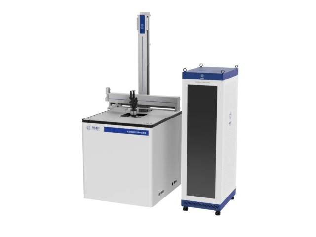
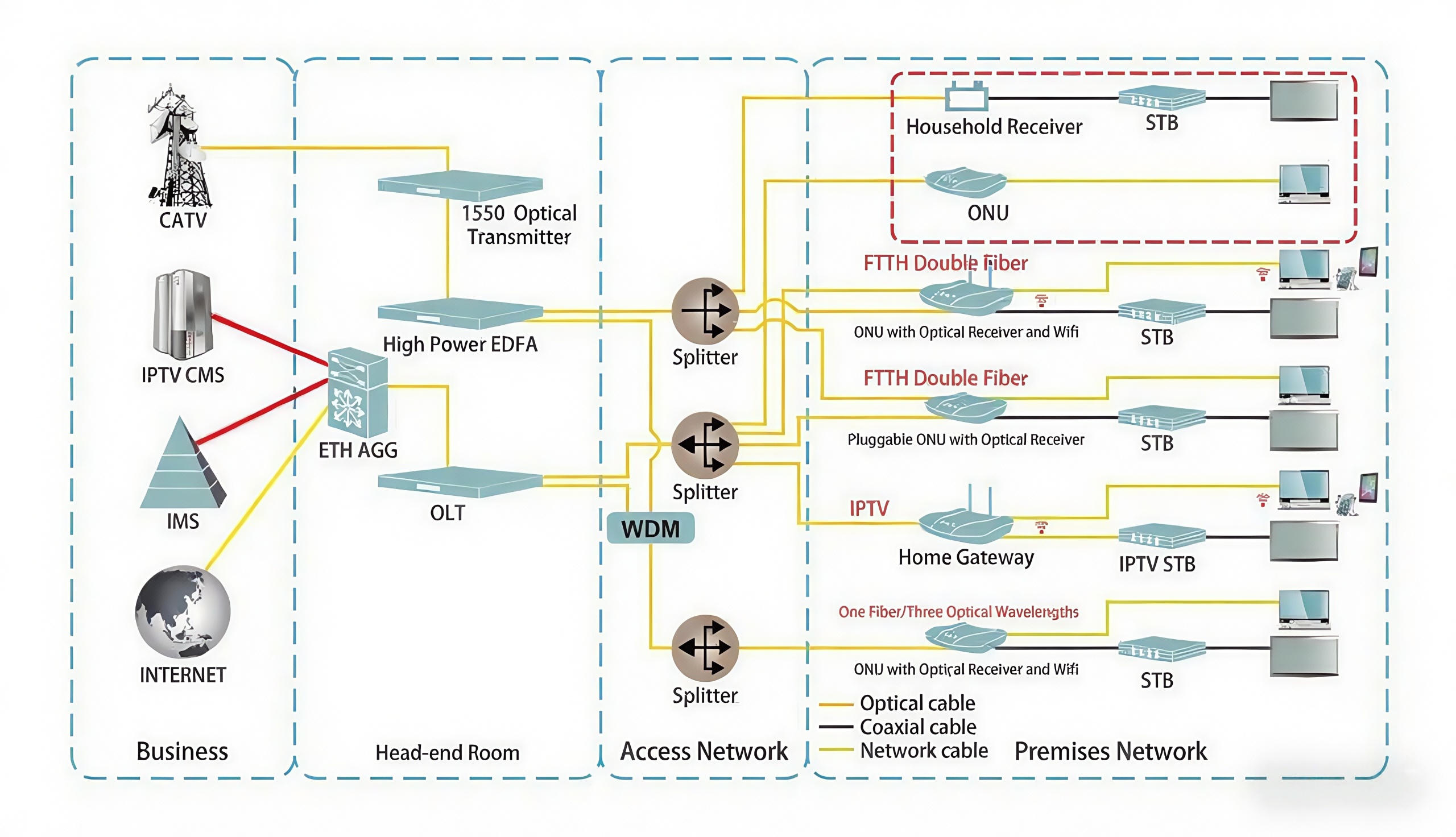
Don’t overlook integration and monitoring. Receivers with integrated high-isolation WDM + PIN reduce BOM and space while simplifying 1550 nm video overlay alongside data wavelengths. Extras like I²C access, optical power/RF level/temperature telemetry, and RF enable/disable make field diagnostics faster and enable smarter ONUs. Sanland’s SMO-P42 illustrates this integration approach and is designed expressly for FTTH ONU use in triple-play deployments.

Why SANLAND for your next CATV optical receiver? Beyond competitive specs, SANLAND backs its CATV Optical Receiver Module line with a one-stop FTTx portfolio and experience dating back to 2002—meaning faster selection, cohesive interoperability, and mature manufacturing. The product range spans AGC receivers for GPON/XGS-PON and options positioned for customization (e.g., Custom AGC / Customizable cable TV module), so you can match noise, linearity, connectors, and control interfaces to your design without wrestling with multi-vendor compromises. Pair that with responsive engineering support and a focused fiber-access roadmap, and you get a SANLAND-branded Low Noise Optical Receiver or High-Performance CATV AGC Module that ships with both performance confidence and service reliability.

For many universities, national labs, and research institutes in regions such as Africa and the Middle East, access to advanced scientific instrumentation is often limited by budget, infrastructure, and maintenance challenges. Scanning Electron Microscopes (SEMs) are essential tools for materials science, life sciences, and education, but traditional models can be prohibitively expensive and difficult to maintain.

This is why affordable SEM solutions have become critical for resource-limited environments. But "affordable" should not mean compromising on performance or usability. Below, we explore the key factors to consider when selecting a cost-effective SEM and how CIQTEK is helping research communities worldwide overcome these challenges.


Why Resource-Limited Labs Need Affordable SEMs

In developing regions, researchers often face unique barriers:

  • Budget Constraints – High upfront costs and ongoing maintenance make many SEMs inaccessible. 

  • Infrastructure Limitations – Power supply stability, room conditions, and service availability can restrict choices.

  • Educational Demands – Universities need SEMs that are easy to learn, operate, and maintain for student training.

  • Service and Support Gaps – Remote locations often lack local technical support, making reliability and remote assistance crucial.

For example, a university in East Africa wanted to give engineering students access to SEM imaging. A million-dollar instrument was out of reach, but a cost-effective, compact SEM made it possible to expand their curriculum and attract new research collaborations; A national lab in the Middle East struggled with power fluctuations that frequently disrupted their older high-end SEM. Switching to a robust, lower-maintenance system ensured consistent imaging and reduced downtime.


What to Look for in an Affordable SEM

When evaluating SEM options for resource-limited labs, consider the following:

  • Total Cost of Ownership
    Not just the purchase price, factor in maintenance, consumables, and energy use.

  • Ease of Use
    A user-friendly interface helps reduce training costs and allows students and new researchers to get hands-on quickly.

  • Durability & Reliability
    Instruments should perform consistently even in less-than-ideal lab conditions.

  • Remote Support & Training
    For institutions far from service centers, remote diagnostics, online training, and virtual demonstrations are essential.

  • Scalability
    SEMs should be versatile enough to support both teaching and research, making them a long-term investment.


CIQTEK SEM: Affordable Without Compromise

At CIQTEK, we’ve worked with institutions worldwide to deliver SEMs that combine affordability with reliability. Our systems are designed for teaching labs, national facilities, and emerging research groups that need dependable performance without excessive cost.

  • Budget-Friendly Pricing – Enables universities and labs to invest in advanced imaging while leaving room for consumables, training, or lab expansions.

  • Low Maintenance Design – Reduced service needs mean fewer interruptions and lower long-term costs.

  • User-Friendly Interface – Ideal for classrooms, making SEM operation accessible to undergraduates and postgraduates alike.

  • High-Quality Imaging – Clear results suitable for materials science, biology, and applied engineering research.


Whether for a teaching university in Africa or a national lab in the Middle East, CIQTEK SEMs provide a reliable and affordable choice that empowers scientific discovery.

CIQTEK SEM microscope


>> If you’re looking for a cost-effective SEM, contact CIQTEK today to learn how our SEM instruments can support your research and teaching needs.

Recently, a team led by Wang Haomin from the Shanghai Institute of Microsystem and Information Technology of the Chinese Academy of Sciences made significant progress in studying the magnetism of zigzag graphene nanoribbons (zGNRs) using a CIQTEK Scanning Nitrogen-vacancy Microscope (SNVM).


Building on previous research, the team pre-etched hexagonal boron nitride (hBN) with metal particles to create oriented atomic trenches and used a vapor-phase catalytic chemical vapor deposition (CVD) method to controllably prepare chiral graphene nanoribbons in the trenches, obtaining ~9 nm wide zGNRs samples embedded in the hBN lattice. By combining SNVM and magnetic transport measurements, the team directly confirmed its intrinsic magnetism in experiments. This groundbreaking discovery lays a solid foundation for the development of graphene-based spin electronic devices. The related research findings, titled "Signatures of magnetism in zigzag graphene nanoribbons embedded in a hexagonal boron nitride lattice," have been published in the prestigious academic journal "Nature Materials".


Graphene, as a unique two-dimensional material, exhibits magnetic properties of p-orbital electrons that are fundamentally different from the localized magnetic properties of d/f orbital electrons in traditional magnetic materials, opening up new research directions for exploring pure carbon-based magnetism. Zigzag graphene nanoribbons (zGNRs), potentially possessing unique magnetic electronic states near the Fermi level, are believed to hold great potential in the field of spin electronics devices. However, detecting the magnetism of zGNRs through electrical transport methods faces multiple challenges. For instance, nanoribbons assembled from the bottom up are often too short in length to reliably fabricate devices. Additionally, the high chemical reactivity of zGNR edges can lead to instability or uneven doping. Furthermore, in narrower zGNRs, the strong antiferromagnetic coupling of edge states can make it difficult to detect their magnetic signals electrically. These factors hinder direct detection of the magnetism in zGNRs.


ZGNRs embedded in the hBN lattice exhibit higher edge stability and feature an inherent electric field, creating ideal conditions for detecting the magnetism of zGNRs. In the study, the team used CIQTEK's Room-Temperature SNVM to observe the magnetic signals of zGNRs directly at room temperature.


Figure 1: Magnetic measurement of zGNR embedded in a hexagonal boron nitride lattice using Scanning Nitrogen-vacancy Microscope


In electrical transport measurements, the fabricated approximately 9-nanometer-wide zGNR transistors demonstrated high conductivity and ballistic transport characteristics. Under the influence of a magnetic field, the device exhibited significant anisotropic magnetoresistance, with a magnetoresistance change of approximately 175 Ω at 4 K, a magnetoresistance ratio of about 1.3%, and this signal persisted even at temperatures as high as 350 K. Hysteresis was only observed under a magnetic field perpendicular to the plane of the zGNRs, confirming its magnetic anisotropy. Through analysis of the variation of magnetoresistance with tilting angle, the researchers found that the magnetic moment is perpendicular to the sample surface. Furthermore, the decrease in magnetoresistance with increasing source-drain bias and temperature revealed the interaction between magnetic response and charge transport and thermal vibrations.


Figure 2: Magnetic transport characteristics of 9-nanometer-wide zGNR devices embedded in hBN


This research, by combining Scanning Nitrogen-vacancy Microscope technology and transport measurements, directly confirmed the existence of intrinsic magnetism in hBN-embedded zGNRs for the first time, providing a possibility for controlling magnetism through an electric field. This work not only deepens the understanding of graphene's magnetic properties but also opens up new pathways for the development of spin electronic devices based on graphene.


Experience the Nano-scale Magnetic Imaging System


CIQTEK invites you to experience the Scanning Nitrogen-vacancy Microscope (SNVM) – a globally leading nano-scale magnetic field imaging system, operating at temperatures of 1.8~300 K with a vector magnetic field of 9/1/1 T, achieving a magnetic spatial resolution of 10 nm, and magnetic sensitivity of 2 μT/Hz1/2.


SNVM is a precision measurement instrument that combines Diamond Nitrogen-vacancy (NV) Optically Detected Magnetic Resonance (ODMR) technology with Atomic Force Microscopy (AFM) scanning imaging technology. It features high spatial resolution, high-sensitivity magnetic imaging, versatile detection capabilities, and non-invasive detection advantages, making it important in areas such as magnetic domain characterization, antiferromagnetic imaging, superconductor characterization, and research on two-dimensional magnetic materials.

Room temperature version of SNVM

Cryogenic version of SNVM


Beyong Nano, a leading innovator in nanotechnology, is set to unveil its groundbreaking model CIQTEK SEM3200 at the prestigious 33rd International Materials Research Congress taking place in Cancun, Mexico.


The Congress, known for bringing together pioneers and visionaries in the field of materials science, provides Beyong Nano with the perfect platform to showcase CIQTEKlatest technological marvel.


The Scanning Electron Microscope is poised to revolutionize the industry with its advanced features, unparalleled performance, and potential applications across various sectors. 


Visitors to the Beyong Nano booth at the congress can experience firsthand the transformative potential of the model 3200 and engage with the company's team of experts to learn more about its features, applications, and future developments.

We, CIQTEK, are pleased to invite you to the Electron Microscopy Conference 2025, held from October 13th to 15th, 2025, at the Theodor Bilharz Research Institute, Egypt. 


The theme of this year's conference is: "The Importance of Electron Microscopy in Enlightening the Invisible". It reflects the profound impact that electron microscopy continues to have across diverse scientific disciplines, from biology to materials science.


Over the conference's three days, we will have the opportunity to engage in in-depth tutorials, keynote sessions, and explore the latest technological advancements in the field of Electron MicroscopesIt will follow a Hybrid format, allowing participants from around the world to join us both in person and virtually, ensuring an inclusive and accessible experience for all.


Meet us at ESEM

Date: October 13 - 15, 2025


LocationTheodor Bilharz Research Institute, Egypt


In the use of smart sports watches, users often face some frustrating issues:

  • GPS drift: running tracks appear inaccurate or offset;
  • Unstable Bluetooth: frequent disconnections with phones or earbuds;
  • High power consumption: battery drains too fast, limiting usage time.

These problems are not solely caused by software. A key factor lies in the crystal oscillator (XO) selection during hardware design.

Crystal Oscillator Solutions for Sports Watches

The Role of Crystal Oscillators

Crystal oscillators serve as the precise clock source for the GPS module, Bluetooth chip, and MCU controller inside sports watches.

  • For GPS: even a tiny clock error can lead to significant location drift.
  • For Bluetooth: frequency deviation may cause connection loss or data errors.
  • For power management: unstable clocks reduce efficiency in low-power modes, draining the battery faster.

Root Causes of Common Issues

  1. Low-accuracy oscillators → large temperature drift, poor stability in varying environments
  2. Insufficient power optimization → faster battery drain.
  3. Lack of differential/temperature-compensated solutions → poor performance in outdoor environments.

JGHC Crystal Oscillator Solutions

For sports watches and wearable devices, JGHC recommends:

Conclusion


When your sports watch suffers from inaccurate GPS, unstable Bluetooth, or short battery life, the true reason might be that the wrong crystal oscillator was chosen.

JGHC Crystals is committed to providing high-precision, low-power, and highly reliable oscillator solutions for wearable devices, helping brands deliver superior user experiences.


For more crystal oscillator application solutions, please contact JGHC.

The basic working principle of quartz crystal oscillator

Quartz crystal oscillators utilize high-quality piezoelectric crystals, harnessing the piezoelectric effect to generate stable oscillations. The crystal's quality factor (Q) directly impacts frequency stability—a higher Q provides a more accurate and reliable clock signal. The vibration frequency characteristics are determined by three key factors: crystal thickness, crystal geometry, and cutting method.


Effect of thickness on frequency

The frequency of a quartz crystal is inversely proportional to the thickness of the crystal:

Thin wafers: Support higher oscillation frequencies, ideal for high-frequency applications.

Thick wafers: small vibration amplitude and excellent resistance to mechanical shock

Technological breakthrough : Overtone crystal technology enables a chip with a fundamental frequency of 20MHz to reach 100MHz through the fifth overtone, allowing medium and low fundamental frequency chips to meet high-frequency requirements of hundreds of megahertz.


Chip shape and frequency characteristics


Tuning Fork Chip

Typical application: 32.768kHz crystal oscillator

Typical dimensions: 3.2 × 1.5 × 0.8 mm

Temperature characteristics: parabolic characteristics of -0.04ppm/℃²

Manufacturing process: Photolithography technology is used to achieve micron-level precision

Frequency determining factors: mainly depends on the fork length (L), the longer the length, the higher the frequency

Advantages: Especially suitable for low-frequency precise timing scenarios


Fectangular Wafer

Frequency range: MHz level application

Miniaturization: From 7.0×5.0mm to 1.6×1.2mm

High frequency: Up to 300MHz through chamfered edge technology

Low power consumption: current consumption can be as low as 0.5μA

Main features: convenient for large-scale production and standardized packaging

Frequency Determinants: Thickness is the Main Influencing Factor


Comparison of key cutting technologies

The cutting angle of the quartz crystal (defined in the XYZ coordinate system) directly affects:

(1) Long-term aging characteristics

(2) Temperature stability

(3) Frequency accuracy

Mainstream cutting methods : AT cutting, BT cutting, SC cutting, IT cutting, and special cutting processes designed specifically for tuning fork wafers. Each method has its own performance advantages and applicable scenarios.


Contact

Need the optimal quartz crystal oscillator solution for your application? Our team of engineers can provide complete crystal oscillator selection recommendations and technical support, from low to high frequencies, based on your specific application needs.

Please contact our sales team:  

Tel: 0086-576-89808609  

Email: market@acrystals.com

Website: [www.acrystals.com](http://www.acrystals.com)  

What Makes Rogers RT/duroid 5870 Laminates Ideal for High-Frequency Electronics and Precision Circuits?


In the demanding landscape of high-frequency electronics, Rogers 5870 laminates stand as a pinnacle of engineering excellence. These PTFE-based composites, reinforced with randomly dispersed glass microfibers, deliver unparalleled dielectric consistency—making them the substrate of choice for precision stripline and microstrip circuitry. Engineered to thrive in broadband and high-frequency environments, RT/duroid 5870 Material minimizes signal dispersion and energy loss while extending operational efficiency into the Ku-band and beyond.


Critical Performance Attributes

1.Ultra-Low Dielectric Properties

With a dielectric constant (Dk) of 2.33 and dissipation factor (Df) of 0.0012 (verified at 10 GHz),Duroid 5870 PCBensures minimal signal delay and attenuation. These properties enable high-speed signal integrity for 5G infrastructure, satellite communications, and phased-array radar.


2.Moisture Resistance for Harsh Environments

Leveraging inherent PTFE characteristics, the material exhibits remarkably low moisture absorption (0.02%). This resilience guarantees stable performance in high-humidity conditions—critical for avionics, maritime systems, and tropical deployments.


3.Unmatched Signal Integrity

As the lowest-loss reinforced PTFE material available,Rogers RT/Duroid 5870 provides isotropic behavior with uniform electrical properties across all axes. This eliminates directional performance variances, ensuring consistent impedance control for multi-layer RF designs.


RT duroid 5870 pcb features


Advanced PCB Manufacturing Capabilities

We deliver end-to-end solutions for Duroid 5870 High Frequency PCB-based circuits, supporting the most complex high-frequency applications:


Structural Versatility

Layer Configurations: Single-layer, double-layer, multi-layer (up to 24 layers), and hybrid stacks combining FR-4/Rogers materials.

Thickness Range: Standard options from 10 mil to 62 mil, including 15 mil, 20 mil, and 31 mil profiles. Custom thicknesses available.

Panel Scalability: Maximum panel size of 400mm×500mm—ideal for large-format antennas or multi-project arrays.


Surface Engineering

Copper Weights: 1oz or 2oz finished copper with±0.07 mil tolerance. 

Solder Masks: Green, black, blue, red, yellow, and matte finishes.

Surface Finishes:

Immersion Gold (ENIG)

HASL (Lead/Lead-free)

Immersion Silver/Tin

ENEPIG (for wire bonding)

Electrolytic Hard Gold

OSP & Bare Copper


Rogers 5870 PCB Capability


Mission-Critical Applications

Rogers 5870’s blend of electrical stability and environmental endurance makes it indispensable across defense, aerospace, and telecom sectors:


  • Aerospace: Airborne broadband antennas, collision avoidance systems.
  • Military: Radar arrays, missile guidance PCBs, electronic warfare modules.
  • Telecom: Point-to-point radio antennas, millimeter-wave backhaul links.
  • Emerging Tech: Automotive radar (77/79 GHz), quantum computing interconnects.


 RT/duroid 5870 high frequency PCBs


Why Partner with Us?

As an ISO 9001-certified supplier, we combine Rogers material expertise with:


  • Impedance Control:±5% tolerance via TDR testing.
  • Hybrid Bonding: Seamless integration of RT/duroid 5870 with FR-4/ceramics.
  • High-Tg Processing: Lamination cycles optimized for PTFE’s low thermal expansion.
  • DFM Support: Signal layer adjacency planning and via optimization.


Industry Challenge Solved: Traditional FR-4 laminates suffer from erratic Dk values above 6 GHz. RT/duroid 5870’s glass microfiber matrix eliminates this variability—enabling precise phase matching in 40 GHz beamforming networks.


Conclusion

For engineers pushing the boundaries of high-frequency design,RT/duroid 5870 high frequency PCBs deliver uncompromised signal fidelity, thermal resilience, and manufacturing flexibility. Whether developing next-gen radar or satellite payloads, this material system bridges the gap between theoretical performance and real-world reliability.

What Makes RT/duroid 6002 the Premier Choice for Demanding High-Frequency PCB Applications?


In the relentless pursuit of performance within the RF and microwave sector, the selection of printed circuit board (PCB) substrate material is a critical determinant of success. For engineers designing cutting-edge systems where signal integrity, thermal management, and reliability are non-negotiable, Rogers Corporation's RT/duroid 6002 laminates emerge as a superior microwave material solution. This advanced composite, engineered with ceramic-filled polytetrafluoroethylene (PTFE), is specifically formulated to meet the rigorous demands of complex microwave structures, offering an unparalleled blend of electrical and mechanical properties that guarantee exceptional performance and longevity in multi-layer board constructions.


Exceptional Material Properties for Peak Performance

The standout characteristics of Rogers 6002 laminates are rooted in their precise and stable electrical properties, which are meticulously tailored for high-frequency applications.


Rogers 6002 features


1.Consistent Dielectric Constant:

With a dielectric constant (Dk) of 2.94 and an exceptionally tight tolerance of±0.04, these laminates provide a stable electrical environment that is paramount for impedance control. This consistency is vital for maintaining signal integrity, minimizing reflection, and ensuring predictable performance across the entire board.


2.Superior Thermal Stability:

A common challenge in high-frequency applications is performance drift caused by temperature fluctuations. The Rogers RT/duroid 6002 addresses this with an ultra-low thermal coefficient of dielectric constant (12 ppm/°C). This ensures that the Dk value remains stable over a broad temperature range, safeguarding the electrical performance of your design against thermal variations and ensuring operational consistency in diverse environments.


3.Minimal Signal Loss:

The dissipation factor (loss tangent) is a crucial metric for efficiency. At a remarkably low value of 0.0012 at 10 GHz, RT/duroid 6002 exhibits minimal electrical energy loss, converting it into heat. This translates to highly efficient transmission of microwave signals, reduced attenuation, and enhanced overall signal quality, which is essential for long-range and sensitive communication systems.


4.Enhanced Mechanical Reliability:

Beyond electrical performance, the laminate’s low Z-axis coefficient of thermal expansion (CTE) of 24 ppm/°C is a key feature for structural integrity. This characteristic signifies outstanding dimensional stability, drastically reducing the risk of warping, delamination, or plated through-hole failure when the board is subjected to thermal cycling during assembly and operation. This inherent stability is a cornerstone for building reliable, high-layer-count multilayer boards.


Advanced PCB Manufacturing Capabilities for RT/duroid 6002

Leveraging the superb properties of this material requires a manufacturing partner with precise expertise. Our specialized PCB fabrication services are optimized to fully harness the potential ofRogers RT/duroid 6002 material, offering extensive flexibility to meet your exact design requirements.


RT/duroid 6002 PCB Manufacturing Capabilities


1.Layer Configuration Versatility:

We support a comprehensive range of structures, from simple 1-layer and 2-layer boards to sophisticated multi-layer and hybrid designs that incorporate other materials for optimized cost and performance.


2.Customizable Construction: 

To achieve target impedances and manage current loads, we accommodate standard copper weights of 1oz (35µm) and 2oz (70µm). Furthermore, we provide a selection of precise PCB thicknesses, including 10mil (0.254mm), 20mil (0.508mm), 30mil (0.762mm), 60mil (1.524mm), and 120mil (3.048mm).


3.Larger Format Boards: 

Our production capabilities can accommodate PCB sizes up to 400mm x 500mm, providing ample real estate for larger, more complex circuitry often found in advanced radar and antenna systems.


4.Finishing Options:

We offer a variety of solder mask colors (Green, Black, Blue, Yellow, Red, etc.) and a complete suite of surface finishes. These include Bare Copper, HASL, ENIG, Immersion Silver, Immersion Tin, pure Gold (directly on copper), ENEPIG, and OSP, ensuring optimal solderability and protection for your specific application.


RT/duroid 6002 High Frequency PCBs


Broad-Ranging Applications

The unique combination of electrical and mechanical properties makes RT/duroid 6002 High Frequency PCBs the material of choice for a wide array of critical, high-performance applications. These include:


-Phased Array Antennas

-Ground-Based and Airborne Radar Systems

-Global Positioning System (GPS) Antennas

-High-Speed Power Backplanes

-Commercial Airline Collision Avoidance Systems


Conclusion

For designers pushing the boundaries of RF and microwave technology, the substrate is not just a foundation—it's an active component of the system's performance. Rogers RT/duroid 6002 substrates, with their proven low-loss, stable Dk, and outstanding reliability, provide the technical excellence required for next-generation applications. Partner with a supplier that possesses the advanced manufacturing capabilities to transform this exceptional material into a high-precision, reliable PCB that will elevate your product's performance. Contact us today to discuss your project requirements and discover how our expertise can benefit your next high-frequency design.


Why Choose RO3003 High Frequency PCBs for Stable RF/Microwave Performance?


Introduction

RO3003 high-frequency laminates represent a breakthrough in advanced circuit materials, engineered to deliver unparalleled electrical performance, mechanical resilience, and economic efficiency. As a ceramic-reinforced PTFE (polytetrafluoroethylene) composite, these laminates provide a superior solution for demanding microwave and RF applications. Their ability to maintain consistent signal integrity across extreme frequencies positions Rogers RO3003 as an indispensable material for next-generation technologies.


In environments where thermal and frequency fluctuations challenge conventional materials, Rogers RO3003 PCB excels with its remarkably stable dielectric constant. This stability is critical for automotive radar systems operating at 77 GHz, millimeter-wave 5G infrastructure, and Advanced Driver Assistance Systems (ADAS), where precision signal propagation directly impacts safety and functionality. By minimizing phase shifts and impedance variations, Rogers 3003 laminates ensure reliable performance in mission-critical applications.


Electrical & Mechanical Properties


ro3003 features


2.1 Precision Dielectric Characteristics


  • Dk Stability: With a dielectric constant (Dk) of 3.00±0.04 across temperature and frequency ranges, RO3003 enables predictable impedance control essential for high-frequency designs.


  • Ultra-Low Signal Loss: A dissipation factor of 0.0010 at 10 GHz minimizes insertion loss, preserving signal strength in mmWave applications up to 77 GHz and beyond.


2.2 Thermal Reliability


  • Minimal CTE Variation: CTE values of 17 ppm/°C (X-axis), 16 ppm/°C (Y-axis), and 25 ppm/°C (Z-axis) prevent delamination and via cracking during thermal cycling.
  • Thermal Consistency: Maintains electrical properties from -50°C to +150°C, ideal for automotive underhood electronics and outdoor RF infrastructure.


2.3 Quality & Cost Efficiency


  • ISO 9001-Certified Manufacturing: Guarantees batch-to-batch consistency and compliance with international quality standards.
  • Budget Optimization: Delivers RF performance comparable to premium laminates at 30–40% lower cost, reducing BOM expenses without sacrificing reliability.


 RO3003 BENEFITS


Advanced PCB Manufacturing Capabilities for RO3003

To fully leverage RO3003 High Frequency PCB’s properties, our manufacturing processes ensure precision and flexibility:


RO3003 Manufacturing Capabilities


Layer Count Versatility:

We accommodate diverse design complexities, expertly manufacturing Single Sided, Double Sided, Multi-layer PCBs (including complex HDI designs), and Hybrid constructions combining RO3003 with other specialized materials for optimal performance and cost management.


Flexible Copper Weights: 

Tailor current carrying capacity and trace characteristics with standard options like 1oz (35µm) and 2oz (70µm) copper foil, with custom weights available to meet specific RF and thermal requirements.


Precise Dielectric Thickness Control:

Achieve the exact impedance and performance targets with a wide range of dielectric thicknesses, spanning from a thin 5mil (0.127mm) up to a robust 60mil (1.524mm).


Generous Panel Sizing:

Our production capacity supports PCB panels up to 400mm x 500mm, efficiently handling larger boards or optimizing panelization for smaller components.


Solder Mask Options: 

Maintain brand identity or functional needs with a selection of solder mask colors, including Green, Black, Blue, Yellow, Red, and others.


Comprehensive Surface Finishes: 

Ensure optimal solderability, wire bonding capability, shelf life, and signal integrity by choosing from our full range of surface finishes:


  • Immersion Gold (ENIG)
  • Hot Air Solder Leveling (HASL - Leaded or Lead-Free)
  • Immersion Silver
  • Immersion Tin
  • Electroless Nickel Electroless Palladium Immersion Gold (ENEPIG)
  • Organic Solderability Preservative (OSP)
  • Bare Copper (for specific controlled environments)
  • Pure Gold (Hard Gold) for edge connectors or demanding wear applications.


 Rogers 3003 pcb


Critical Applications Leveraging RO3003

1. Automotive Radar Systems:

77 GHz long-range radar (LRR) and short-range radar (SRR) sensors for adaptive cruise control and collision avoidance.

Low moisture absorption (<0.1%) ensures performance in humid environments.


2. 5G Infrastructure:

mmWave base station antennas (24–43 GHz) requiring stable Dk across temperature gradients.

Massive MIMO arrays with ultra-low loss feed networks.


3. Aerospace & Telecommunications:

GPS/GNSS satellite antennas with precise phase stability.

5G NR small cells and remote meter readers operating in harsh outdoor conditions.


4. High-Power RF Systems:

Power backplanes and military-grade radar utilizing Z-axis CTE stability for plated-through-hole reliability.


Conclusion

RO3003 high frequency PCBs bridge the gap between cutting-edge electrical performance and manufacturability. With industry-leading Dk stability, minimal loss characteristics, and rigorous quality certification, this laminate empowers designers to push the boundaries of 77 GHz automotive radar, 5G mmWave, and ADAS innovations. Partner with us to access full-spectrum manufacturing capabilities—from rapid prototyping to complex hybrid stacks—tailored to your application’s unique demands.