Step into a new era of wearable technology with theM02C Smart Glasses from North Edge. Designed for daily commuting, travel, and social interaction, these smart glasses combine style, comfort, and intelligence in one lightweight device. Weighing only 41g, the ergonomic design and soft silicone nose pads allow you to wear them all day without discomfort. The ultra-elastic hinges and flexible temple arms further enhance a seamless fit.
At the heart of M02C is a powerful 800W HD camera with Sony 219 chip, offering first-person photography and 1080P video recording. Dual image stabilization ensures every shot is clear, while images and videos can be easily transferred via WiFi. Pair with Bluetooth for high-quality audio recording, immersive music playback, and crystal-clear calls, making your smart glasses a versatile multimedia companion.
The AI voice assistant lets you interact hands-free: instant image recognition, real-time translation, and barrier-free chatting allow effortless communication across 139 languages. Whether you say “Hey Cyan”, the smart glasses respond promptly. The glasses are powered by a 290mAh battery with magnetic charging, giving up to 7 hours of usage and quick 2-hour recharge.
Built to handle daily challenges, the M02C is IP65 waterproof and sweat-proof, ready for outdoor use in diverse conditions. Whether capturing memories, staying connected, or exploring new horizons, the M02C smart glasses integrate health, communication, and entertainment seamlessly.
Discover the convenience, style, and cutting-edge AI of North Edge M02C Smart Glasses, and bring the universe into view at your fingertips.
In this blog, we introduce the new North Edge FORTRESS outdoor watch through a short product video. The footage was recorded during our internal product preparation process, showing the watch in real conditions.
The video mainly introduces the core features and design of the North Edge FORTRESS, including:
Case structure and rugged design
Button operation and menu navigation
Screen clarity and outdoor visibility
Overall appearance and wrist feel
All footage was taken from real samples prepared for wholesale supply, without studio rendering or post-production effects.
FORTRESS is a newly introduced outdoor watch model from North Edge, developed for users who require durability and clear functionality in outdoor environments.
Application: Hiking, camping, everyday outdoor use
Supply model: Wholesale distribution
Real Product, Real Stock
The product shown in the video is the same version supplied to our wholesale partners. We share real product footage to help distributors better understand the actual condition of the watch before placing bulk orders.
Wholesale Availability
FORTRESS is currently available for wholesale orders. North Edge supports stable stock supply and long-term cooperation with distributors worldwide.
👉 For wholesale pricing, MOQ, and lead time, please contact our sales team.
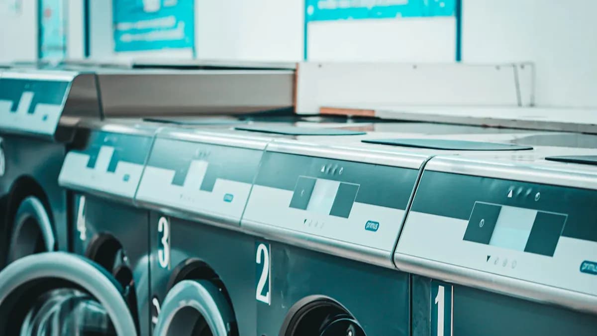
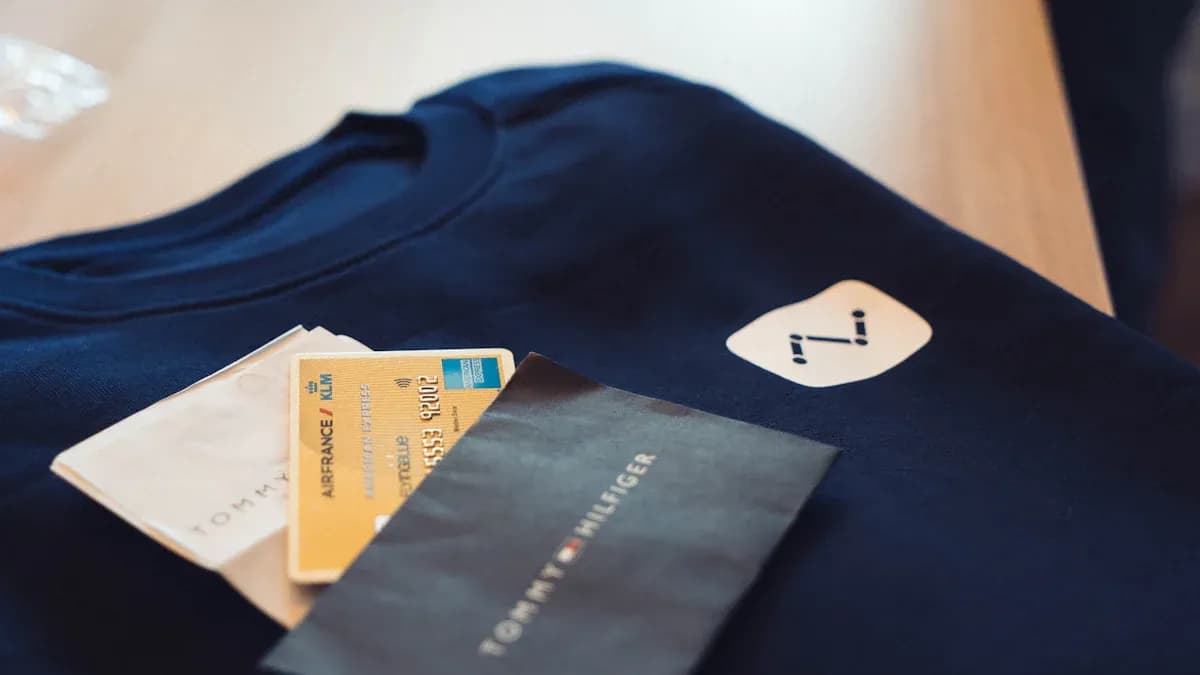
If you’re looking to make laundry easier and less stressful, RFID laundry tag technology is the solution you need. By using an RFID laundry tag, you can quickly track and sort clothes, streamlining your entire process. The Wholesale Price RFID UHF Laundry Tag provides a smart and cost-effective way to upgrade your laundry routine.
See how RFID laundry tag technology compares to traditional methods:
Method
Setup Cost Range
Labor Savings
ROI Timeframe
RFID
$3,000–$5,000
Saves 15–20 hours weekly
7–9 months
Barcode
$1,200–$1,800
N/A
N/A
With RFID laundry tag solutions, you benefit from fast sorting, fewer lost items, and peace of mind every time you wash.
Key Takeaways
RFID laundry tags make sorting and tracking clothes easier. They help you save time and make fewer mistakes.
Using RFID technology helps stop items from getting lost. This gives you peace of mind and makes customers happier.
Buying RFID tags can save a lot of work for businesses. It can help companies get their money back fast.
Pick strong RFID tags that can handle tough laundry jobs. This will help them last a long time.
Good training and care for RFID systems make them work better. This helps laundry management be more accurate and fast.
RFID Laundry Tag Benefits
Sorting and Tracking Made Easy
Laundry should be easy and not stressful. RFID technology helps with this. When you use an rfid laundry tag, sorting and tracking clothes is simple. You just scan to check your clothes. This works at home or in a business. RFID tags use radio waves to find each item fast. You do not have to scan every piece alone. You can scan a whole cart at once. This saves time and stops mistakes.
Here is a table that shows how rfid tags make sorting and tracking better:
Feature
Description
Fast and accurate identification
RFID helps you find each piece quickly and exactly.
Simultaneous tag reading
You can scan many clothes at the same time.
Live reporting
RFID gives you updates about washing and inventory right away.
Durable and weatherproof
RFID tags work after many washes and in tough places.
RFID pocket tags help you keep track of all your clothes. You always know where your items are. This helps you avoid mix-ups.
Preventing Lost Items
Losing clothes is stressful and costs money. RFID laundry tag solutions help stop this. With rfid, you can scan all your linens or uniforms together. You can track items inside and outside your laundry. Hotels and hospitals lose fewer items after using rfid.
RFID lets you scan a whole cart of linens fast.
You can track items by route, customer, or place.
One big hotel chain lost 20% fewer linens with rfid.
RFID pocket tags help you count and track every item. This makes you feel better and keeps customers happy.
Saving Time and Effort
RFID tags for laundry save you time every day. You do not need to count or sort by hand. RFID readers scan tags from far away. You can check inventory in seconds. This helps you finish laundry faster and with less work.
Increased Efficiency: RFID makes sorting and tracking quicker, so you do less work.
Inventory Management: You can check inventory fast and find lost items quickly.
Automated Reporting: RFID systems make reports for you, so managing is easier.
Here is how it works:
Register each clothing item with its type and owner.
Put an rfid laundry tag on each item.
Use an RFID reader to scan and track items as they move.
RFID technology also makes things more accurate. Experts say rfid makes accuracy go from 65% to over 95%. This means fewer mistakes and better results.
Built for Harsh Environments
You need rfid tags that last through many washes and tough places. The High Temperature Laundry Rfid Tag is made for this. It uses PPS material and is waterproof with IP68 rating. It can handle over 200 industrial washes and very hot or cold temperatures. This tag works even in hard laundry jobs.
Feature
Specification
Material
PPS (Polyphenylene Sulfide)
Waterproof Rating
IP68
Wash Cycles
200+ industrial washes
Working Temperature
-20°C to +180°C
High-Temperature Resistant
Up to +220°C
You can trust these rfid laundry tags to last and work well, even in big laundry places.
Better Inventory Management
RFID tags for laundry help you manage inventory easily. You can track every item, make fewer mistakes, and keep customers happy. Here are some benefits:
Benefit
Explanation
Streamline asset tracking and accountability
RFID tags help you track items, so you always know where things are.
Reduce manual errors and increase accuracy
Automatic counts mean fewer mistakes and better control.
Improve customer satisfaction with reliable service
Real-time data helps you avoid lost items and delays, so customers trust your service.
RFID technology gives you the info you need to run laundry smoothly. You get updates right away and can make better choices.
Tip: If you want to make laundry better, try rfid laundry tag solutions. They make sorting, tracking, and inventory easy and reliable.
Cost-Effective Laundry Tag Solutions
Home vs. Business Use
You want laundry to be easy and not stressful. RFID technology helps you do this. At home, rfid pocket tags help you track your family’s clothes. You scan clothes fast and stop mix-ups. In businesses, rfid makes sorting and tracking much quicker. Hotels, hospitals, and laundromats use rfid for thousands of linens each day. You save time and make fewer mistakes.
Tip: Pick rfid laundry tag solutions that fit your laundry size and needs. You get better results when you choose the right tag for your items.
Here is a table that shows how rfid changes labor costs in commercial laundry:
Impact Area
Description
Labor Cost Reduction
Automation of linen tracking reduces manual handling and human error, leading to lower labor costs.
Improved Operational Efficiency
Enhanced workflow efficiency and reduced turnaround time due to automated processes.
Inventory Management
Real-time data on stock levels and garment location improves accuracy and reduces scrap rates.
Wholesale and Bulk Options
You want to save money and get good value. Buying rfid tags in bulk saves you more over time. The Wholesale Price RFID UHF Laundry Tag is a smart pick for big orders. You get strong tags for less money. Businesses can upgrade their laundry system without spending too much.
When you pick rfid tags, think about these things:
Durability: Choose tags that last through many washes and resist chemicals.
Installation Methods: Decide if you want to sew or heat-seal the tags.
Reading Distance and E-Performance: Make sure the tags work well in your laundry area.
Know the size and type of laundry items you have.
Think about washing conditions, like hot water.
Make sure the tags work with your laundry management system.
You get more control and better info with rfid. You can track every item and always know where your linens are. RFID laundry tag solutions help you run laundry smoothly and keep your customers happy.
RFID Laundry Tags: Limitations
Cost and Investment
You want laundry to be easier with rfid. The first cost can look high. You pay for tags, readers, and setup. Over time, you save money. You lose fewer items and spend less on labor. Many businesses get their money back in a year. RFID gives you more control and better results. The starting price is worth it for most people.
Durability Concerns
RFID laundry tags need to last through tough washes. Some tags break after many cycles. Problems include cracked paint, bent copper wire, and faded particles. These issues can make tags stop working after 30 washes. Here is a table that shows these problems:
Tag Model
Durability Issue
Result After 30 Cycles
M1
Conductive paint cracks
Non-functional
M2
Copper wire deforms
Non-functional
M3
Conductive particles dissipate
Non-functional
You want tags that handle heat, chemicals, and water. Good rfid pocket tags last over 250 washes and up to 3 years. Some advanced tags survive more than 1,000 washes and very hot or cold temperatures. You get strong performance when you pick the right tag.
Privacy and Data
You care about your privacy and information. RFID makes tracking laundry easy, but you must keep data safe. Anyone with a reader can scan rfid tags. Someone could see private info if you do not protect your system. Risks include people getting data without permission, stealing data during transmission, messing with devices, and stopping the system from working. Here is a table that shows privacy risks:
Risk Type
Description
Unauthorized Access
People could get sensitive data from rfid tags.
Data Interception
Data can be stolen while moving between tags and readers.
Device Tampering
Someone could change or steal data by touching rfid devices.
System Disruptions
Problems could stop rfid systems from working right.
You can keep data safe by using secure readers and controlling who can scan. You feel better when you protect your information.
Tip: Pick rfid laundry tag solutions that are strong and secure. You get better results and keep your privacy safe.
Getting Started with RFID Laundry Tags
Choosing the Right Tag
You want laundry to be simple and work well. First, pick rfid laundry tags that fit what you need. Choose tags that match the clothes or linens you wash. Think about where you use them. Busy hotels or hospitals need tags that last through many washes and high heat. At home, pick tags that are easy to put on and bend. Make sure the tag works with your laundry system. Put the tag in the right spot to stop mistakes and help tracking. It is important to teach workers how to scan and use tags. Check your system often and talk with your team to find problems early.
Tip: Training and good tag use stop 25% of laundry mistakes. Make sure everyone knows how to use rfid.
Maintenance Tips
You want your rfid laundry tags to last a long time. Follow these easy steps:
Wipe tags with a soft cloth or gentle cleaner to keep them clean.
Keep tags away from too much heat, water, and sunlight.
Do not let tags touch strong chemicals.
Try not to scan or write data too much to avoid damage.
Pick strong tags for hard jobs.
Always do what the maker says.
These tips help your rfid tags work well and keep laundry easy.
Long Range Ucode8 UHF RFID Laundry Tag
If you need to scan lots of items or from far away, the Long Range Ucode8 UHF RFID Laundry Tag is a good pick. This tag works well for busy laundry places. It is flexible, strong, and scans from far away. Here is what makes it special:
Feature
Description
Ultra-thin
Bends to fit many things
Wash Cycle Durability
Lasts over 200 washes
Long Range
Reads tags from 1 to 6 meters
High Temperature Resistance
Works in hot places
Waterproof
Handles wet laundry easily
You can change the size, add barcodes, and trust the tag to handle folding and chemicals. With rfid, you can track every item from start to finish. You stop losing things, make fewer mistakes, and grow your business with less worry. Planning and following rules is easier with rfid.
Note: Use rfid tags that fit your laundry needs. You get better results and feel less stressed.
You can use rfid to make laundry easier and more reliable. It helps you sort clothes faster and track them better. You will lose fewer items when you use rfid. Many people say they save money and see their inventory better. Tracking can be almost perfect, up to 99% right. There are some problems, like learning how to use new systems. You also need to make sure all parts work together. If you have lots of laundry or need to scan from far away, try the Long Range Ucode8 UHF RFID Laundry Tag. This tag gives you the best results.
Main benefits:
Sorting and tracking are much faster
You lose fewer items
Inventory is more accurate
Limitations:
You need training
You must set up the system
Make laundry less stressful by using smart rfid solutions.
FAQ
How do you attach an RFID laundry tag to clothing?
You can sew, heat-seal, or insert the tag into a pocket on your clothing. This keeps the tag secure during washing. You will not lose track of your items.
Will RFID laundry tags survive many washes?
Yes, these tags are built for tough laundry cycles. You can wash, dry, and iron your clothes without worry. The tag stays strong and keeps working.
Can you use RFID laundry tags at home?
You can use rfid laundry tags at home for family clothes. You will sort and find items faster. This makes laundry day simple and stress-free.
Do RFID laundry tags work with all fabrics?
Most rfid laundry tags work with cotton, polyester, and blends. You can use them on uniforms, linens, and towels. Always check the tag’s instructions for best results.
How do RFID laundry tags help prevent lost items?
You scan each item with a reader. The system tracks every piece from start to finish. You will always know where your clothes are.
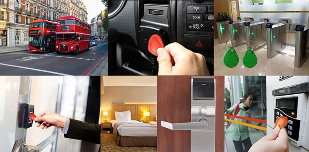
You get better security with near field communication key fobs. They use strong encryption and two-way communication. Secure access is important for buildings, vehicles, and devices. Radio frequency identification technology, like RFID Key Fobs, helps control entry for offices, cars, and devices. Here are some common uses:
Use Case
Description
Building Access
Key fobs let people enter buildings without keys. They help control who goes in and out.
Vehicle Security
Fobs let you lock or unlock cars from far away. You can start engines without regular keys.
Device Authentication
Key fobs work as security tokens for devices. They make sure only approved users can get in.
NFC tags help with smart home entry.
You can use them as digital keys in your phone wallet.
Key Takeaways
NFC key fobs are safer than RFID key fobs. This is because they use strong encryption and talk both ways. - RFID key fobs are good for outside or tough places. They are strong and can handle bad weather. - NFC key fobs are best for fast entry in offices and smart homes. You can also use your phone as a key with them. - Always pick key fobs that have strong encryption. This helps stop copying and keeps out people who should not get in. - Keep checking your access systems to make sure they stay safe from new dangers.
RFID Key Fobs Security Features
How RFID Key Fobs Work in Access Control Systems
RFID key fobs help you open doors and gates. You do not need a regular key. When you put the fob close to a reader, it sends a special code. The code travels by radio waves. The system checks the code to see if you can go inside. Many RFID key fobs use high-frequency chips like 13.56 MHz. These chips have more features. You see RFID access control in offices and hotels. Parking lots use these systems too. They help control who can enter each area.
Security Mechanisms in RFID Key Fobs
RFID key fobs keep your things safe with many protections:
Encrypted RFID systems keep your data safe when sent.
Many RFID key fobs use symmetric encryption to keep messages secret.
Some systems use mutual authentication. The fob and reader check each other first.
High-frequency RFID key fobs have extra security and better encryption.
These protections make it hard for someone to copy or hack your fob. You can trust RFID key fobs to protect your building or device.
Durability and Environmental Resistance
RFID key fobs are made to last in tough places. Many fobs resist water and dust. They can handle very hot or cold weather. Some tags work even with strong acids or chemicals. You can use them outside or in factories. Look for fobs with high ingress protection ratings like IP65, IP66, or IP69K. These ratings mean better water resistance. Some RFID key fobs work at 200°C or -190°C.
Mechanism Type
Description
Physical Tamper Evidence
Fobs break or show warnings if opened.
Data-Level Protection
Encryption locks or deletes data if tampered.
Dual Tamper Protection
Uses both physical and data security for more safety.
RFID key fobs work well even in harsh places.
NFC Key Fobs Security Features
How NFC Key Fobs Work in Access Control Systems
You use nfc key fobs by tapping them near a reader. The fob and reader send signals to each other. This only works when they are very close together. You can find nfc access control in homes, schools, and offices. These systems let you open doors or log in to computers. You can also pay for things with a tap. You do not need to swipe or insert anything. The system checks who you are. If you have permission, you get access. This makes nfc access control quick and safe.
Security Protocols in NFC Key Fobs
Nfc key fobs use strong rules to keep your data safe. They use encryption to hide your information every time you use them. The fob and reader share secret codes that change each time. This makes it hard for someone to steal your data.
To stop relay attacks, systems use special security steps. These include secure authentication, encryption, and safe key exchange. For example, codes or tokens can change every time you try to get in. This helps block attackers from tricking the system.
You get more safety because both the fob and reader are checked. This two-way check helps stop hackers from copying your key fob.
Versatility and Application Scenarios
Nfc key fobs work in many places and ways. You can use them in hospitals to keep patient areas safe. They help protect private information. Staff can get in easily, which keeps everyone safe.
You can set up nfc access control for small offices or big companies. This means you get the right security for your needs.
Nfc systems work well with other security tools. You can see who enters in real time. You can also change who gets in quickly if needed.
Nfc key fobs give you a safe and flexible way to control access almost anywhere.
RFID vs NFC: Security and Encryption
Data Transmission and Encryption Standards
You want your key fob to keep your info safe. How data moves and gets locked is important for this. When you use rfid, your key fob sends info to a reader with radio waves. The signal can travel a few feet away. This makes it simple to use, but someone could try to catch the signal. NFC key fobs only work when you hold them very close to the reader, just a few inches away. This short distance helps keep your info safe.
Encryption makes your info hard to read for others. Both rfid and NFC can use strong locks, but NFC often uses better ones like AES-128. This keeps your info safe even if someone tries to listen. You can see the main differences in the table below:
Feature
RFID
NFC
Operational Range
A few feet
A few inches
Vulnerabilities
Prone to cloning and electromagnetic interference
Requires smartphone access for security
Authentication
Generally one-way communication
Enables two-way communication
Key Card Requirement
Physical key cards needed
Smartphones can act as key cards
Maintenance
More maintenance due to physical cards
Low maintenance with cloud integration
Tip: Pick a key fob with strong locks for better safety in your access control systems.
Authentication and Two-Way Communication
Authentication checks if you are allowed to enter. In rfid systems, the reader sends a signal to the key fob. The fob answers with its code. This is called one-way talking. It works well, but it can be less safe. Someone could try to copy the code if they get close.
NFC key fobs use two-way talking. The reader and the fob talk to each other. Both sides check if the other is real. This makes it much harder for someone to trick the system. You get more safety because both devices must agree before you get in.
Here is a quick look at important ways to talk safely:
Protocol Type
Description
Data Encryption
Makes sure stolen data cannot be read by others.
Secure Communication
Sends data safely so people cannot listen in.
Note: Two-way talking in NFC helps stop hackers from copying or replaying your key fob.
Physical and Digital Security Differences
You need to think about both body and digital safety. rfid key fobs are tough and can handle hard places. They can resist water, dust, and even chemicals. This makes them good for outside or factory use. NFC key fobs are also strong, but their main power is in digital safety.
For digital safety, NFC gives you more protection. The short range and two-way checks make it harder for someone to steal your info. rfid can be easier for attacks like copying or catching signals. You can lower these risks by picking rfid key fobs with locks and keeping your system up to date.
If you want the best safety for your access control, look for key fobs that are both strong and have good digital locks. This way, you stay safe in every situation.
Vulnerabilities: How to Duplicate an RFID Key Fob and Other Risks
Common Attacks on RFID Key Fobs
You may wonder how to duplicate an RFID key fob. Attackers use several methods to duplicate your fob and gain access to secure places. The most common attack is cloning. In this attack, someone uses a cloner to copy the data from your fob. They can then create a duplicate that works just like your original. Some attackers use an RFID cloner kit, which can read and copy the code from your fob in seconds. These kits are small and easy to hide.
Here are the main ways attackers duplicate RFID key fobs:
Cloning attacks create fake copies of real RFID tags. These copies can trick readers and open doors.
Attackers use a cloner to scan your fob without you knowing. They only need to get close to your pocket or bag.
Some RFID key fob types have weak security. Attackers target these types because they are easier to duplicate.
Limitations in the size and cost of RFID tags can make them less secure.
You should know that not all RFID key fob types are the same. Some use better encryption and are harder to duplicate. Others are more basic and easier for a cloner to copy.
Common Attacks on NFC Key Fobs
NFC key fobs also face risks, but the attacks are different. To duplicate an NFC key fob, an attacker needs to get very close to your fob. The short range makes it harder to use a cloner. Most NFC systems use strong encryption and two-way checks. This means both the reader and the fob must agree before opening a door.
Still, some attacks can happen:
Hackers may try to intercept the signal if they get close enough.
Attackers may use a cloner, but they need special tools and must be right next to you.
Some older NFC key fob types may not have the latest security features.
You can lower your risk by choosing NFC key fobs with advanced encryption. Always update your access control systems to block new threats.
Cloning, Hacking, and Real-World Threats
You may ask how to duplicate an RFID key fob in real life. Attackers often use a cloner or an RFID cloner kit. They scan your fob, copy the code, and make a duplicate. Some people try to duplicate an apartment key fob to get a spare for friends or family. Others use a service that promises to make a spare, but this can be risky if you do not trust the service.
Real-world incidents show the risks of weak RFID key fob types. For example, attackers used SDR devices to capture signals from Hitag2 key fobs. They broke the 48-bit cipher and cloned keys in less than a minute. This led to many car thefts.
Incident Description
Method of Exploitation
Outcome
Hitag2 Key Fob Vulnerability
Attackers use SDR devices to capture transmissions and exploit a 48-bit cipher
Keys can be cloned in under a minute, leading to vehicle thefts
You can protect yourself from these threats. Here are some tips:
Use RFID-blocking wallets or pouches. These stop a cloner from scanning your fob.
Choose RFID key fob types with advanced security features. Some can disable your car’s ignition or track its location.
Add extra layers to your access control systems. Use alarms or immobilizers with your fob.
Update your software often. This keeps your system safe from new attacks.
Do not use a service you do not trust to duplicate your fob or make a spare.
If you need a spare, always use a trusted service. Never share your fob with someone you do not know. You can lower your risk by staying alert and using the right tools.
Tip: Always check if your RFID key fob types use strong encryption. If you use an RFID cloner kit or a service to duplicate your fob, make sure you follow safe practices.
When you compare RFID and NFC, you see that NFC key fobs are harder to duplicate. The short range and strong encryption help protect you. RFID key fob types with weak security are easier for a cloner to copy. You should always choose the best technology for your needs and keep your access control systems up to date.
Practical Considerations for Access Control Systems
Ease of Use vs Security in RFID and NFC Key Fobs
You want a key fob that is easy to use and keeps your property safe. RFID and NFC key fobs both offer simple ways to unlock doors or devices. You only need to tap or hold the fob near a reader. However, you should think about how each type works in daily life.
The table below shows the main factors that affect ease of use for both types:
Feature
NFC
RFID
Read Range
Very short range, typically up to 4 cm.
Varies from a few centimeters to several meters.
Data Transfer
Quick two-way communication.
Typically one-way data transmission.
Ideal Use Cases
Contactless payments, quick file transfers.
Large-scale inventory management, asset tracking.
Integration
Commonly found in smartphones.
Requires specialized readers, less integration with smartphones.
You may find NFC key fobs easier if you want fast, secure entry and use with your phone. RFID key fobs give you more range, which helps in parking lots or warehouses. Always check compatibility with your current system before choosing a key fob. If you want both ease of use and strong security, look for products with advanced encryption and mutual authentication.
Cost, Implementation, and Customization
You need to think about cost when you set up access control systems. The price can change based on the type of key fob and the size of your project. Here is a quick look at the cost range for each system:
System Type
Cost Range
RFID
$1,500 - $3,500
NFC
$2,000 - $4,500
RFID systems often cost less to start, especially for large buildings. NFC systems may cost more, but they give you extra features like phone integration and two-way security checks. You should also check compatibility with your doors, gates, or devices before you buy.
Customization matters if you want your key fobs to match your brand or special needs. OEM RFID Factory lets you add your logo or choose special shapes and colors. For example, the Plus S 2K 13.56MHz RFID Key Tag offers logo printing and engraving. The ABS NFC Keyfob supports eco-friendly materials and works with Amiibo, making it a smart choice for gaming or payment systems.
Choosing the Right Key Fob for Your Needs
When to Choose RFID Key Fobs
Pick RFID key fobs if you need something tough. They work well outside and in hard places. These fobs are good for gates, parking lots, and factories. They can handle water and chemicals. RFID key fobs are great for big groups of people. You can use them for hotels, worker badges, or warehouse doors. They let you open doors from far away. These fobs also have strong locks to stop copying.
Tip: Use RFID key fobs if your area has bad weather or lots of use. You can trust them to last a long time.
When to Choose NFC Key Fobs
Choose NFC key fobs if you want fast and safe entry. They work best in offices, schools, and smart homes. NFC fobs check both the reader and the fob. This makes it harder for hackers. You can use your phone as a key with NFC. This makes things easier for you. NFC is good for small groups or if you want to pay with your fob. You can also use them for games or tickets.
Note: NFC key fobs give you strong digital safety and easy daily use.
Advanced Options: RFID Key Tag and ABS NFC Keyfob
You can get more safety with special types like the RFID Key Tag and ABS NFC Keyfob from OEM RFID Factory. These fobs have extra features for places that need more security. The table below shows what makes them special:
Feature
Description
Durability
ABS material keeps the fob strong in tough places.
Waterproof
Special sealing stops water from getting in.
Advanced Security
AES or 3DES locks make copying very hard.
Compliance
Works with many systems because it meets ISO rules.
Anticollision Function
Many fobs can work at once without losing data.
These fobs help keep your building safe from threats. They are good for hotels, offices, and special jobs. If you want something strong and safe, pick these for your next upgrade.
You get stronger security with NFC key fobs because they use advanced encryption and two-way checks. Real-world reports show that both RFID and NFC can have risks, so you need to identify your fob type and stay updated. You should review faqs about rfid key fob types before you order the matching rfid cloner kit or always keep a spare. Choose the right key fob for your needs. In retail and warehouses, RFID helps with security by tracking items and stopping theft. Explore OEM RFID Factory’s solutions for the best fit.
FAQ
What makes NFC key fobs more secure than RFID key fobs?
You get better security with NFC key fobs because they use two-way communication and strong encryption. These features help you control who enters your space. NFC systems also require close contact, which lowers the risk of signal theft.
Can someone easily duplicate my RFID key fob?
You face risks if your RFID key fob uses weak encryption. Attackers can use a cloner to copy your fob. You should choose advanced RFID key fobs with strong encryption to control access and keep your systems safe.
How do I choose the right key fob for my access control systems?
You should look at your environment and security needs. Use RFID key fobs for outdoor or industrial control. Pick NFC key fobs for offices or smart homes. Always check if your systems support advanced encryption and mutual authentication for better control.
Are RFID and NFC key fobs waterproof and durable?
You can find both RFID and NFC key fobs that resist water and harsh weather. Many products use ABS material for extra strength. This helps you control access in tough places and keeps your systems working well.
What should I do if I lose my key fob?
You need to tell your control manager right away. They can remove your lost fob from the system. This stops others from using it. Good systems let you add or remove fobs quickly, so you keep control over who enters.
You find the Blank Rfid Card in Escape from Tarkov as a rare and mysterious item. This card appears important because you need it for a specific quest in the game. Many players wonder about its true purpose, which adds to its intrigue.
Key Takeaways
The Blank RFID Card is essential for completing the 'The Ticket' quest in Escape from Tarkov. Keep it safe until you turn it in to progress in the game.
You can find the Blank RFID Card in marked rooms on the Reserve map. Focus on these areas to increase your chances of finding this rare item.
The card has a high market value, often selling for over 1,000,000 ₽. If you don't need it for a quest, consider selling it for a significant profit.
Stay active in the Escape from Tarkov community to learn about potential new uses for the Blank RFID Card. Developers may introduce new features in future updates.
Always check the latest patch notes for changes in item spawn locations. This can help you find the Blank RFID Card more efficiently.
Blank RFID Card Overview
In-Game Description
You will see the Blank Rfid Card described as a personalized RFID card with a strict design. The card looks almost exactly like Kruglov's keycard, but the owner's name has been scrubbed off on purpose. This card gives you access to the TerraGroup evacuation point, which only trusted personnel can use. The mysterious nature of this card makes many players curious about its true purpose in Escape from Tarkov.
Appearance and Rarity
When you find a Blank Rfid Card, you notice its black, unmarked surface. The card does not have any visible writing or logos. This simple look makes it stand out from other keycards in the game. You will not see this card often. It is one of the rarest items you can find in Escape from Tarkov. Many players spend hours searching for it because of its value and importance.
Tip: If you spot a black, blank card in a loot room, check it carefully. It could be the Blank Rfid Card you need.
Where to Find
You can find the Blank Rfid Card in a few special places. The most common spot is inside marked rooms on the Reserve map. These rooms often have high-value loot, but they are also dangerous because other players want the same items. Sometimes, you might find the card in other high-tier loot areas, but Reserve marked rooms give you the best chance. Always check safes, lockers, and special containers when you search these locations.
Reserve marked rooms
High-value loot containers
Safes and lockers
Finding the Blank Rfid Card takes patience and luck. You improve your chances by learning the best spawn points and moving quickly through dangerous areas.
Blank RFID Card Uses
Quest Requirement
You need the Blank Rfid Card for a key quest called "The Ticket" on the Mr. Kerman storyline. This quest asks you to deliver the card to complete an important objective. Many players struggle to find this card because it is rare. When you bring the card to the quest giver, you unlock new tasks and progress further in the story. The quest does not let you use any other card, so you must find the correct one. You should keep the card safe until you finish the quest.
Note: If you lose the Blank Rfid Card before turning it in, you must search for another one. This can slow down your progress in Escape from Tarkov.
Hideout and Crafting Potential
Some players believe the Blank Rfid Card could have uses in the hideout, especially in the intelligence center. You might see rumors about crafting recipes or upgrades that need this card. Right now, the game does not let you use the card for crafting or hideout upgrades. Developers may add new features in the future. You should watch for updates and patch notes. If the card becomes part of a recipe, you will want to know right away.
Here is a table showing possible future uses:
Area
Potential Use
Status
Intelligence Center
Crafting recipes
Not available
Hideout Upgrades
Special access
Not available
Quests
Turn-in item
Confirmed
Speculated Functions
Players often discuss what else the Blank Rfid Card might do. Some think it could open secret doors or unlock new areas. Others guess it might work with future events or rare loot containers. The community shares ideas on forums and social media. You can join these discussions to stay informed. Sometimes, developers listen to player feedback and add new features. You should keep the card if you find one, even after finishing the quest. It might become more valuable later.
Tip: Stay active in the Escape from Tarkov community. You will hear about new uses for the Blank Rfid Card as soon as they appear.
Value and Player Strategies
Market Value
You will notice that the Blank Rfid Card holds a high value in the Escape from Tarkov player market. Many players want this card because it is rare and needed for quest progression. If you find one, you can sell it on the flea market for a large amount of in-game currency. The price often changes based on how many cards are available and how many players need them for quests. You should check the market before selling to get the best price.
Item
Average Price (₽)
Demand Level
Blank Rfid Card
1,000,000+
Very High
Other Keycards
200,000-800,000
Medium
Tip: If you do not need the card for a quest, selling it can give you a big boost in money.
Progression Importance
You must have the Blank Rfid Card to complete "The Ticket" quest. This quest is important for moving forward in the Mr. Kerman storyline. Without the card, you cannot finish the quest or unlock new missions. Many players get stuck at this point because they cannot find the card. You should keep the card safe until you turn it in. Do not risk losing it in raids.
Tips for Finding and Using
You can improve your chances of finding the card by focusing on Reserve marked rooms. These rooms have a higher chance to spawn rare items. Move quickly and check all loot containers. Play with friends to cover more ground and protect each other. If you find the card, place it in your secure container right away. This keeps it safe even if you die.
Learn the best spawn points on Reserve.
Use offline raids to practice routes.
Watch for updates that may add new spawn locations.
Note: Always check the latest patch notes. Developers sometimes change where rare items spawn.
You now understand why the Blank Rfid Card matters in Escape from Tarkov. You need it for quests, and you can sell it for a high price. Many players want this rare item. You should keep watching for updates because new uses may appear. Stay active in the community to learn more.
FAQ
What does the Blank RFID Card look like?
You see a black card with no markings or logos. The surface appears smooth and plain. This design makes it easy to spot among other keycards.
Where can you find the Blank RFID Card most often?
You usually find the card in marked rooms on the Reserve map. High-value loot containers and safes also have a chance to spawn it. You need patience and luck.
Can you use the Blank RFID Card for crafting or hideout upgrades?
Not right now. The game does not allow you to use the card for crafting or hideout upgrades. Developers may add new uses in future updates.
What should you do if you find a Blank RFID Card?
Place it in your secure container.
Keep it safe until you finish the quest.
Check the flea market for current prices if you want to sell.
CIQTEK is pleased to announce its participation in the French EPR Society Meeting – ARPE Days 2026, taking place March 19–20, 2026, at Chimie ParisTech in Paris, France. The event brings together researchers, instrument specialists, and industry partners from across Europe to exchange the latest advances and practical applications in Electron Paramagnetic Resonance (EPR).
A Key Meeting Point for the EPR Community
ARPE Days serves as an important annual gathering for the French and broader European EPR community. The meeting provides a platform for discussing developments in magnetic resonance methods, new experimental approaches, and real-world research applications across chemistry, physics, materials science, energy research, and life sciences.
For CIQTEK, the event is also an opportunity to reconnect with long-standing collaborators and meet new researchers exploring advanced EPR solutions for their laboratories.
Over the past few years, CIQTEK EPR spectrometers have been successfully delivered to multiple leading research organizations and universities across Europe, supporting work in free radical studies, catalysis, battery research, materials characterization, and quantum-related investigations.
At ARPE Days 2026, visitors will be able to learn more about CIQTEK's growing EPR portfolio, including:
Benchtop EPR systems, offering compact, cost-effective solutions for routine measurements and teaching labs
Pulse EPR systems supporting more sophisticated spin dynamics and structure investigations
Q-band and W-band EPR solutions for higher resolution and sensitivity in cutting-edge research fields
Supporting accessories and upgrades, including temperature control and application-driven configurations
In addition to new systems, CIQTEK also provides EPR modernization and upgrade solutions, enabling laboratories to extend the lifetime and capabilities of existing instruments through electronics, control system, and performance upgrades without requiring full instrument replacement.
Real Applications, Real Labs
Researchers interested in practical use cases can also explore , where laboratories worldwide share how EPR is being used to solve real research challenges.
From energy materials to catalytic mechanisms and paramagnetic defect analysis, these stories highlight how EPR moves beyond theory into everyday lab impact. Visitors and readers are encouraged to explore the EPR Customer Stories section on the CIQTEK website to see how different research groups are applying the technology.
Meet CIQTEK in Paris
CIQTEK looks forward to engaging with the EPR community in Paris, exchanging ideas, and exploring future collaborations!
For more information or to schedule a meeting during the event, feel free to contact the CIQTEK team in advance.
From delivering stable power and data transmission for construction machinery operating in harsh environments, to safeguarding the reliable performance of wind turbines, energy storage systems, and ultra-high-voltage power grids, WAIN heavy-duty connectors are engineered for mission-critical applications. From connectors and bus I/O modules enabling efficient collaboration on industrial automation lines, to stable power delivery and high-speed interconnect solutions supporting data centers and artificial intelligence, WAIN integrates reliable connectivity into every essential scenario.
Within the critical systems of rail transportation, WAIN’s modular designs support high-speed and dependable operation. In marine and offshore energy development, robust sealing and durability ensure protection in demanding deep-sea conditions. WAIN’s high-voltage connection systems power the electric drive cores of new energy vehicles, while its charging solutions provide convenient and efficient energy replenishment for sustainable mobility. Lightweight, high-speed connectors further enable advanced aerial platforms to achieve greater efficiency and performance.
From wind turbines rising hundreds of meters above the ground to precision contacts measured at the nanometer scale, connectivity is everywhere. WAIN remains committed to delivering reliability where it matters most, empowering every critical system with dependable connection solutions.
In industrial wiring and equipment protection applications, the sealing reliability and installation adaptability of bulkhead interfaces are often critical challenges. To address this, WAIN introduces the W Series bulkhead connector housing, providing a structurally robust and installation-flexible standard solution for cable entry and exit sealing in control cabinets and equipment enclosures.
1
Design Features: Extended Structure for Dual-Side Protection
The W Series adopts a longitudinally extended bulkhead design, where part of the housing extends into the interior of the cabinet, allowing a cable gland to be installed at the inner end. This structure ensures that both the exterior and interior sides of the enclosure achieve the same level of sealing and protection, preventing internal exposure to condensation, dust, moisture, or mechanical interference. As a result, connection stability is improved throughout the entire product lifecycle.
2
Front and Rear Installation Options for Different Assembly Conditions
The main body of the W Series bulkhead housing features a symmetrical front-and-back structure, supporting two installation methods:
●Front-panel installation (fastened from outside the cabinet to the inside)
●Rear-panel installation (fastened from inside the cabinet to the outside)
Users can select the most convenient installation direction based on cabinet structure, cable routing direction, and available working space—without modifying the wiring layout due to structural constraints, significantly improving assembly flexibility.
3
Gasket Retention Design: Adhesive-Free, Removable, and Reusable
The sealing gasket is secured to the housing using a snap-fit geometric retention design, eliminating the need for adhesive bonding. Key advantages include:
♦The gasket remains securely in place during installation, reducing the risk of misalignment or detachment
♦Tool-free removal without damage, allowing repeated installation or replacement
♦ The gasket is double-sided and reversible, fully compatible with both front and rear installation orientations
This design balances assembly efficiency with maintenance convenience, making it ideal for applications requiring commissioning, replacement, or future expansion.
4
Models and Sizes Covering Common Wiring Requirements
The W Series bulkhead connector housing is available in multiple sizes, including 6B, 10B, 16B, and 24B, to accommodate different cable quantities and wire diameters. Users can select the appropriate housing size and thread interface based on actual cable count, cable diameter, and insert specifications.
5
Technical Specifications
Material: Die-cast aluminum
Color: Gray
Locking mechanism: Metal elastic clamping system
Sealing material: NBR
Operating temperature: −40 °C to +125 °C
Flame rating: V0
Protection rating: IP67
6
Typical Applications
Industrial control cabinets and power distribution enclosures (cable entry/exit sealing)
Outdoor cabinets and telecom base stations (waterproof and dustproof interfaces)
Isolation and protection between internal and external equipment connections
New energy applications such as EV charging equipment and photovoltaic junction boxes
·END·
WAIN is not only manufacturing, but also creating!
Any questions and ideas related to industrial connectors,
When you walk into a hotel, lighting shapes your first impression before you even notice the décor. The right hotel lighting welcomes you, sets the mood, and makes you feel at ease. Sunwin Lighting stands out by offering solutions that match your style and meet your guests’ needs, creating spaces that leave a lasting impact.
Lighting Impact on Guest Experience
First Impressions Matter
When you step into a hotel lobby, the lighting greets you before anyone else does. The way a space glows can shape your first impression in seconds. You might notice how the light makes the room feel welcoming or how it highlights the elegant details of a luxury hotel. Good lighting choices help you relax and feel comfortable right away.
Take a look at how different aspects of lighting affect your experience:
Evidence Type
Findings
Visual Comfort
Lighting significantly impacts visual comfort, which is crucial for guests' first impressions. High illuminance reduces fatigue and anxiety.
Color Temperature
Warmer light creates a more positive atmosphere, enhancing guests' feelings of security and relaxation.
Overall Atmosphere
The combination of lighting, color, and decoration style shapes the lobby's atmosphere, influencing guest satisfaction and perceptions.
You want to feel safe and at ease when you arrive. Lighting for hotels plays a big role in that. A bright, well-lit entrance makes you feel secure. Warm tones can make you feel relaxed, while cooler lights might energize you. Here are some ways lighting design in hotel entrances can influence your decisions:
You feel welcome and secure when the lighting is right.
Positive experiences boost your opinion of the hotel brand and can make you want to book again.
Natural light makes spaces feel more inviting.
Rooms without daylight seem unwelcoming, which can lower your interest in booking.
A welcoming atmosphere increases guest satisfaction.
Positive first impressions often lead to higher booking rates.
When you feel secure because of effective lighting, you are more likely to return.
Good visibility adds to a positive guest experience.
Sunwin Lighting understands how important these first moments are. Our hotel lighting programs use modern fixtures and thoughtful designs to create spaces that impress guests from the moment they walk in. You get both style and comfort, making your stay memorable.
Setting the Mood
Lighting does more than just help you see. It sets the mood and creates the ambiance you remember long after you leave. When you walk into a hotel, the lighting can make the space feel cozy, vibrant, or even luxurious. The right lighting choices are key to impacting mood and shaping your overall guest experience.
Here’s how lighting helps set the mood:
Lighting establishes the mood and atmosphere of a space, shaping the overall vibe.
Lighting can evoke emotions, making spaces feel serene, calming, energetic, or lively.
The interplay of light and shadow is essential for crafting the desired ambiance.
Lighting creates a warm and inviting atmosphere for guests as soon as they step into the lobby.
Good lighting enhances the appearance of colors and designs, showing off the beauty of the hotel’s décor.
Hospitality lighting experts know how to use light to create emotional connections with guests.
Color temperature also plays a big part in how you feel. Warm lights create a calming environment, perfect for relaxing after a long day. Cooler lights help you stay alert and focused, which is great for workspaces or active areas. When hotels use the right color temperatures, you feel more positive and comfortable, which can lead to repeat bookings and stronger brand loyalty.
Sunwin Lighting specializes in creating these memorable experiences. Our wide range of products, from LED mirrors to stylish table lamps and ceiling lights, gives you the flexibility to design spaces that match your brand and meet your guests’ needs. We focus on quality and innovation, so you get durable fixtures with modern features like USB charging and power outlets. With Sunwin Lighting, you can transform any hotel space into a place guests love to return to.
Psychological Effects of Hotel Lighting
Mood and Well-Being
Have you ever noticed how your mood changes when you walk into a hotel room with soft, warm lighting? You instantly feel more relaxed and at ease. Lighting does more than just brighten a space. It shapes how you feel and how well you rest. Studies show that when you can control the lighting in your room, like using dimmable lights, you feel less moody and more comfortable. Bright, cool-white light works best during the day in busy areas, while warm lighting helps you unwind in the evening.
Research also points out that sustainable lighting in hotels, especially in beach resorts, boosts your mood and helps you relax. You sleep better and feel less stressed when the lighting creates a cozy atmosphere. Adjustable LED systems let you set the ambiance you want, making your stay more enjoyable. Warm light even helps your body produce melatonin, which means you fall asleep faster and wake up refreshed. Cooler lights keep you alert when you need to focus.
Sunwin Lighting understands how important mood and well-being are for guests. You get access to advanced lighting solutions that let you personalize your space. Our products help you create the perfect ambiance, whether you want to relax after a long day or stay energized for work. With Sunwin Lighting, you can count on a hotel lighting program that supports your comfort and happiness.
Comfort and Safety
You want to feel safe and comfortable every time you walk through a hotel corridor or settle into your room. Lighting plays a huge role in making that happen. Proper lighting improves visibility, which is key for safety in hallways and guest rooms. Soft, ambient lighting gives you a sense of luxury and comfort, making you feel like you’re in a luxury hotel. Well-lit spaces also look cleaner and more spacious, so you feel more at ease.
Here’s how lighting design helps you feel safe and comfortable:
Proper lighting enhances visibility, which is crucial for safety in corridors and guest rooms.
Soft, ambient lighting is associated with luxury and comfort, improving guests' perceptions of the space.
Well-lit areas contribute to a sense of cleanliness and spaciousness, making guests feel more at ease.
Emergency lighting and illuminated pathways guide guests safely during emergencies, reducing panic.
You’ll notice that different areas in a hotel need different lighting strategies. Lobbies use warm, inviting lighting to encourage you to linger, while corridors rely on brighter lights for safe navigation. Accent lighting highlights beautiful design features, adding to the overall ambiance. Warm lighting in guest rooms creates a comforting atmosphere, while brighter lighting in corridors ensures you can move around safely.
Sunwin Lighting excels at creating safe and comfortable environments for guests. Our hotel lighting solutions include emergency lighting, ambient fixtures, and accent lights that work together to make every space feel secure and welcoming. You get high-quality products designed for durability and modern convenience, so you always feel at home.
Key Hotel Lighting Elements
Color and Ambiance
You notice the mood of a space as soon as you walk in. Color temperature plays a big role in shaping that feeling. In hotel lobbies, a warm color temperature between 2700K and 3000K creates a cozy, intimate atmosphere. Bedside lamps in guest rooms often use warmer light for comfort, while desk lamps might be a bit brighter to help you focus. Restaurants feel more inviting with warm lighting, and banquet halls can switch between warm and bright depending on the event.
Lobby Lighting: 2700K–3000K for warmth and intimacy
Guest Room Lamps: 3000K for comfort, 4000K for focus
Restaurant Lighting: 2700K–3000K for a pleasant dining experience
Banquet Halls: Warm for weddings, bright for business events
The colors in a hotel environment also affect how you feel. Warm colors like red and orange make spaces lively and welcoming. Cool colors such as blue and green help you relax. Warm lighting adds comfort, while cool lighting brings calmness and a sense of luxury hotel style.
Brightness and Control
You want to control your environment. Adjustable lighting lets you set the brightness to match your mood or activity. This flexibility improves your comfort, sleep, and productivity. Hotels that use the right color temperature and give you control over brightness see fewer complaints and better guest feedback. You can tailor the lighting to your needs without changing the whole room.
Modern features like USB charging ports and power outlets in lamps make your stay even easier. You can charge your devices right at your bedside or desk. Sunwin Lighting offers these smart solutions, making your experience more convenient and enjoyable.
Layered Lighting
Layered lighting means using different types of lights together. You get ambient lighting for general brightness, task lighting for activities like reading, and accent lighting to highlight special features. This approach creates depth and makes each space feel unique.
Ambient Lighting: Sets the base mood with ceiling lights or chandeliers
Task Lighting: Focused light for reading or working, like LED mirrors or table lamps
Accent Lighting: Highlights artwork or architectural details
Most guests prefer a mix of ceiling lights and table lamps. This combination lets you adjust the ambiance for any activity. Sunwin Lighting’s range—including LED mirrors, wall lamps, and floor lamps—helps you create the perfect layered effect. Our products stand out for their quality, durability, and modern features, making your hotel lighting both beautiful and functional.
Personalization in Guest Room Lighting
Customizing for Preferences
You want your hotel room to feel like your own space. Personalization in hotel lighting lets you adjust the ambiance to match your mood or activity. Many hotels now use smart systems that allow you to control brightness, color, and even the direction of light. You can set warm lights for a cozy evening or switch to bright, cool lights when you need to focus.
Studies show that mood lighting can make guests happier by up to 58%. When you have control over your lighting, you feel more comfortable and satisfied. Here’s a quick look at how personalized lighting impacts your guest experience:
Evidence Type
Description
Mood Lighting Impact
Guests report higher happiness with adjustable lighting.
Personalized Control
Smart systems let you change lights for different activities.
Immersive Environments
Tunable white control helps you focus or relax with different colors.
Hotels use different lighting strategies to meet your needs. You might find presence sensors in your room, like at The Sinclair hotel, which let you adjust lighting levels with a simple touch. Only 23% of guests say they get high levels of personalization, so there’s room for improvement. Sunwin Lighting stands out by offering advanced solutions that help hotels create a tailored experience for every guest. Our products let you control your environment easily, making your stay more enjoyable.
Special Occasions
You want your stay to feel special, especially during important moments like honeymoons or anniversaries. Hotels create memorable experiences by customizing lighting for these occasions. Imagine walking into a room with soft, romantic lighting and beautiful accents. The Grand Hotel on Mackinac Island offers a Grand Romance package with a private sunset candlelit dinner. Ledges Hotel features a Romance by the Falls package, complete with flowers and sparkling wine.
Hotels use accent lighting to highlight flowers or special décor. Ambient lighting sets the mood for celebration. Functional lighting lets you adjust brightness for a cozy dinner or a relaxing evening. Sunwin Lighting helps hotels deliver these experiences with versatile products that support every lighting strategy. You get the perfect ambiance for your special day, making memories that last.
Metric
Description
Guest satisfaction scores
Surveys assess comfort, mood, and style after stays.
Repeat booking rates
Hotels track if improved lighting leads to more returns.
Social media engagement
Guests share photos and comments about lighting and design.
Real-World Hotel Lighting Success
Boutique Hotel Case
Imagine you walk into a boutique hotel where every detail feels intentional. Sunwin Lighting worked with a downtown boutique to upgrade their guest rooms and lobby. The team installed high CRI LEDs, which made colors pop and artwork stand out. You notice the layered lighting approach right away. Ambient ceiling lights set a relaxing tone, while accent lamps highlight unique décor. Guests rave about the cozy atmosphere and the ability to adjust brightness for reading or relaxing. The hotel saw a boost in guest satisfaction scores and more positive reviews online.
Resort Transformation
You might wonder how lighting can change the vibe of a resort. Sunwin Lighting partnered with a coastal resort to revamp their lighting program. The results speak for themselves:
Creates a warm, inviting ambiance that welcomes you from the moment you arrive
Achieves up to 80% energy savings, helping the resort invest in other guest amenities
Reduces maintenance calls because LEDs last longer
Enhances appeal to eco-conscious travelers who value sustainability
The resort now attracts more guests who care about the environment. You feel comfortable knowing the hotel lighting supports both style and sustainability.
Best Practices
If you manage or design hotel spaces, you want to learn from successful projects. Here are some best practices from Sunwin Lighting’s real-world experiences:
Use high CRI LEDs for true color representation
Implement layered lighting to create depth and ambiance
Focus on energy efficiency to lower costs
Hotel managers and designers also share important lessons:
Balancing aesthetics with environmental responsibility matters for facade lighting
Address maintenance challenges early to avoid disruptions
Integrate smart technologies for efficient control
You may face challenges when upgrading lighting systems. Here’s how hotels overcome them:
Challenge
Solution
Initial costs
Conduct thorough cost-benefit analyses
Technological adaptation
Provide continuous education and training
Compatibility issues
Select the right technology partners
When you choose Sunwin Lighting, you get a partner who understands your needs and delivers solutions that elevate guest experiences.
You see how lighting shapes every hotel stay. When you use innovative lighting, you boost guest satisfaction and loyalty. Look at what others have done:
The Santa Marina Hotel in Greece used wireless lighting controls to wow guests right at the entrance.
The Ole-Sereni Hotel in Nairobi added adjustable lighting scenes for better ambiance and comfort.
Sunwin Lighting helps you stand out with custom-made, high-quality products like LED mirrors and table lamps. Our focus on technology and sustainability means you can create unique, memorable spaces for every guest.
FAQ
How does hotel lighting affect your stay?
Lighting shapes your mood and comfort. You feel more relaxed in warm, inviting spaces. Good lighting helps you sleep better and enjoy your room. Hotels use lighting to create memorable experiences for every guest.
Can you control the lighting in your hotel room?
Many hotels offer adjustable lighting. You can change brightness or color to match your mood. Some rooms have smart controls or dimmable lamps. Sunwin Lighting provides modern fixtures that make it easy for you to personalize your space.
What types of lighting fixtures do hotels use?
Hotels use a mix of ceiling lights, table lamps, wall lamps, and LED mirrors. Each fixture serves a purpose. You get ambient light for general comfort, task lighting for reading, and accent lights for style.
Why should hotels choose Sunwin Lighting?
You get high-quality, durable products with modern features like USB charging and power outlets. Sunwin Lighting offers a wide range of stylish options. Our team helps hotels create unique, comfortable spaces that guests love.
Does lighting impact hotel safety?
Yes! Proper lighting keeps hallways and rooms safe. You see clearly and avoid accidents. Emergency lights guide you during unexpected events. Hotels rely on well-designed lighting to protect guests and staff.
Picking the right table lamp for a hotel guest room is crucial for creating a functional, welcoming space that enhances guest satisfaction and encourages positive reviews. Table lamps serve not only as practical task lighting for reading or working, but also as ambient lighting for the room's overall aesthetic. As a leading hospitality lighting supplier, we understand that the right table lamp balances style, scale, and utility while aligning with the hotel's branding, whether it's a luxury, boutique or a modern chain. Here is a guide on how to choose the ideal one for your hotel project.
1. Prioritize Function
The first thing is to see where the lamp will be and what job it needs to do.
* Bedside Lamps: Need to provide a warm ambient glow for relaxing and sufficient illumination for reading. They should be easy to reach from a lying position.
* Desk Lamps: Need to provide focused, bright task lighting for working. Adjustable arms or swivel heads are preferred.
* Side Table Lamps: For both aesthetics and supplemental lighting.
2. Integrate Modern Features
The guests expect modern functionality and convenience.
* Switch: Controls should be intuitive and durable. A well placed, easy-to-find switch is the most welcome option, whether it's a classic on/off rocker switch, a rotary knob, a reliable button, or a modern touch sensor. Try to avoid in-line cord switches which often fall behind the table or socket switches that are troublesome to access.
* Dimmer: Look for lamps with dimmable switches to allow guests to adjust brightness or even change color temperature to set the ideal mood, from bright task lighting for work to soft ambient glows for relaxation.
* Power & USB: Integrated USB-A or USB-C ports, AC outlets, or wireless charging pads in the base are now a premium standard, this's a massive value-add that enables guests to power devices without crawling under desks to find a plug.
3. Match the Room's Overall Decor
The lamp should match the hotel's overall theme and interior design to create a harmony, inviting atmosphere.
* Match the Style: Is your hotel modern, rustic, traditional, or luxury? The lamp's finish, shape, and material should reflect this. A sleek, matte black metal lamp suits a contemporary room, while a ceramic base with a linen shade complements a coastal or Scandinavian aesthetic.
* Achieve Visual Balance: Proportion is key, "The Eye-Level Rule" is a good rule. When a guest sits in bed or at the desk, the bottom of the lampshade should be at or slightly below eye level, so the bulb doesn't glare directly into their eyes. For a bedside table lamp, the height between 26 to 30 inches is standard; For a desk lamp, 22 to 24 inches is usually sufficient. Secondly the lamp should occupy no more than one-third of the nightstand's width. The scale should feel substantial but not obstructing.
* Create Cohesion with Finishes: Tie the room together by matching the lamp's finish to other hardware, such as faucets, door handles, or headboard accents. This creates a curated, intentional look that guests subconsciously appreciate.
4. Ensure Durability
Durability is key in high-traffic hotel environments, so select lamps made from robust materials that can withstand frequent use and cleaning.
* Robust Materials: Opt for materials that resist scratching and are easy to wipe down, such as metals, ceramic, resin, or treated wood. The lamp should feel sturdy, not lightweight or flimsy, to withstand frequent handling.
* Weighted Base: Basically the lamp has a heavy, weighted base. This prevents it from being easily knocked over by guests placing luggage or housekeeping staff cleaning surfaces.
Why Sunwin is Your Ideal Partner for Guest Room Lighting
At Sunwin Hotel Lighting, we provide table lamps that masterfully balance these elements: guest-centric functionality, elegant designs, and commercial-grade quality. We have a wide range of customizable materials, finishes, and shapes to match your unique brand identity perfectly. Contact our lighting specialists today to discuss your project or request samples at sales@sunwinhotellighting.com, we're here for you 7 x 24 hours.