CIQTEK is honored to have participated in the Egyptian Society of Electron Microscopy (ESEM) International Conference 2025, held October 13–15 at the Theodor Bilharz Research Institute (TBRI) in Giza, Egypt. This event convened electron microscopy experts, researchers, and industry representatives from across the Middle East, Africa, and beyond, advancing the frontiers of microscopy in both life sciences and materials research.

This year’s theme, “The Role of Electron Microscopy in Enlightening the Invisible”, resonated across sessions on neuropathology, renal biopsy, infectious agents, nanostructure imaging, and emerging microscopy techniques. TBRI played a central role in organizing the event, in cooperation with Egyptian universities such as Tanta and Assiut.


CIQTEK SEM Advances its Global Footprint at ESEM 2025 in Egypt


CIQTEK’s Contributions & Engagement

At ESEM 2025, CIQTEK showcased its SEM product line, including FIBSEMFESEM, and Tungsten Filament SEM. Our booth drew interest from both biological and materials science researchers, keen to see real-sample imaging, low-voltage performance, and analytical integration.

Beyond exhibits, CIQTEK representatives engaged in technical exchange, discussing how advanced SEM tools can bolster regional research infrastructure. We emphasized our commitment to delivering high-performing instruments, competitive pricing, and local support networks to facilitate adoption in diverse labs across the region.


CIQTEK SEM Advances its Global Footprint at ESEM 2025 in Egypt


Impact & Outlook

The conference underscored how microscopy continues to unveil the unseen—from cellular ultrastructure to nanomaterial phenomena. For many participants, this was a rare opportunity to access a wide spectrum of imaging techniques under one roof, and to converse directly with vendors like CIQTEK.


By engaging with local scientists and institutions, CIQTEK deepens its global reach and contributes to the growth of microscopy in underrepresented regions. We look forward to continuing our support in Africa and the Middle East through instrument installations, training, and responsive service.

Gathering new industrial momentum and leading the future of intelligent manufacturing, the China International Industry Fair (CIIF), a global event in the automation field, will once again bring together top enterprises and cutting-edge technologies to showcase core products and solutions for intelligent manufacturing. We sincerely invite you to join us at this grand event, witness the innovative achievements together, and explore new opportunities for cooperation.


Date: September 23 - 27, 2025
Location: National Exhibition and Convention Center (Shanghai, China)
Booth Number: E023, Hall 5.1


In today’s era of rapid technological development, the performance and reliability of electronic components and devices have become the core focus of attention. This is especially true for devices operating in extreme environments, such as aerospace, automotive engine management, energy equipment, and oil drilling. For these applications, connector standards have reached a new level. In response to these challenges, WAIN Electrical has introduced high-temperature connectors (200℃), designed to maintain performance and reliability under extreme temperature conditions.

WAIN High-Temperature Series Connectors are certified in accordance with the DIN EN 60 664 / DIN EN 61 994 standards.

High-Temperature Series Connectors


Product Advantages

01

High Reliability

Even in extreme temperature fluctuations, WAIN high-temperature series connectors provide stable power transmission and signal conduction.


02

Long Service Life

Made from high-quality materials and rigorously tested, WAIN high-temperature connectors have a long service life, reducing maintenance costs.


03

Strong Applicability

Whether exposed to continuous high temperatures or transient temperature rises, WAIN high-temperature connectors operate normally and are suitable for a variety of complex applications.


04

High Safety

With an IP65/IP67 protection rating, WAIN high-temperature connectors further enhance safety during use.


Technical Parameters

Number of Contacts:6,10,16,24

Rated Current:16A

Rated Voltage:500V

Rated Pulse Voltage:6kV

Contact Resistance:≤1mΩ

Wire Gauge:0.75-2.5mm²(18-14AWG)

Shell Protection Rating:IP65/IP67

Mating Cycles:≥500

Temperature Range:-40℃~+200℃

Contact Material:Copper Alloy

Connection Type:Screw Connection

Contact Plating: Gold/Silver Plating

Insulation Material:LCP

Sealing Component:FPM

Shell Material:Die-Cast Aluminum


China industrial connectors manufacturer


All components of the WAIN high-temperature series connectors (including contacts, inserts, shells, seals, and grounding elements) are designed using high-temperature resistant materials, ensuring the product can operate stably within the specified temperature range.


·END·


WAIN is not only manufacturing, but also creating!

Any questions and ideas related to industrial connectors,

we welcome to discuss with you.


Italy has long been a hub for innovation in materials science, nanotechnology, and cultural heritage preservation. Across the country’s universities and national research centers, scanning electron microscopy (SEM) plays a central role in analyzing microstructures and surface morphologies with high precision. In 2025, the demand for advanced SEM systems in Italy continues to rise, driven by the pursuit of higher resolution, improved automation, and multi-mode analytical capabilities.


SEM as a Core Tool in Italian Research

From the Politecnico di Milano to the National Research Council (CNR) and major materials institutes in Emilia-Romagna, SEM has become indispensable for both academic and industrial research. Italian laboratories rely on these systems to study metals, ceramics, semiconductors, biological samples, and even ancient artifacts.

Recent years have seen a shift from conventional tungsten SEMs to field emission SEM (FE-SEM) platforms, which deliver higher spatial resolution and more stable imaging performance. This evolution reflects the country’s growing focus on nanostructured materials, energy devices, and precision manufacturing — all areas where nanoscale imaging and analysis are crucial.


Performance Priorities for Italian SEM Users

Italian researchers tend to emphasize several practical factors when evaluating SEM systems:

  • Resolution and imaging stability: The ability to observe nanoscale details in materials such as thin films, catalysts, and nanocomposites.

  • Analytical integration: Compatibility with EDS, EBSD, and WDS systems to extract chemical and crystallographic information alongside morphology.

  • Ease of operation and automation: Software-guided imaging and recipe-based workflows are increasingly preferred in multi-user facilities.

  • Temperature and environmental control: In-situ observation of microstructural evolution under heating or vacuum changes is becoming more common.

  • Service and long-term support: Access to local technical expertise and responsive maintenance is a key factor in supplier selection.

These priorities reflect a broader trend: Italian laboratories are modernizing not only their instrumentation but also their workflow efficiency and data reliability.


Modern SEM Systems Entering the Italian Market

In recent years, CIQTEK’s SEM instruments have been increasingly adopted by research and industrial users across Italy. Several systems, including the SEM3200 and SEM3300, have been installed through CIQTEK’s local partner in Rome. It has also established a dedicated CIQTEK SEM demonstration laboratory, where Italian researchers can experience the imaging performance and analytical capabilities of the systems firsthand. These installations highlight the country’s growing interest in high-resolution, stable, and user-friendly SEMs supported by local expertise.

CIQTEK SEM Systems at the Italian Market


A Growing Ecosystem for Advanced Electron Microscopy

Italy’s strong tradition in materials and applied sciences continues to drive demand for advanced electron microscopy. National research centers, universities, and technology companies are jointly shaping a dynamic environment where innovation in imaging and analysis thrives.

With more international suppliers now offering localized support and demonstration facilities, such as CIQTEK’s growing presence through its partner network, Italian users have access to an expanding ecosystem of high-performance, reliable SEM solutions. In addition to advanced imaging quality and stable performance, CIQTEK SEM systems are recognized for their competitive pricing, making high-end field emission microscopy more accessible to a wider range of research and industrial users.

This growing accessibility, combined with strong local technical support, ensures that Italy remains at the forefront of microscopy research and application in Europe, where precision, performance, and affordability converge to empower the next generation of scientific discovery.

CIQTEK has taken another important step forward in Europe with the installation of the SEM4000Pro Field Emission Scanning Electron Microscope (FE-SEM) at the SYNERGIE4 demonstration showroom in France.

The new setup allows researchers and industrial users in Europe to experience high-resolution imaging, analytical performance, and ease of operation offered by the CIQTEK SEM4000Pro. The system provides outstanding image quality for fine microstructural observation and supports a wide range of applications in materials science, microelectronics, and R&D.


SYNERGIE4 is CIQTEK's French distributor and service provider for advanced microscopy and microanalysis solutions. With extensive experience in electron microscopy and analytical instruments, SYNERGIE4 supports universities, research institutes, and industrial labs across France with tailored solutions, technical expertise, and training.

Now, SYNERGIE4’s demo center features a fully operational CIQTEK SEM4000Pro, offering hands-on demonstrations for visitors to explore its imaging capabilities, intuitive software interface, and versatility across various research fields.


“Having the CIQTEK SEM4000Pro available in our showroom allows us to showcase its imaging performance directly to our customers,” said a representative from SYNERGIE4. “It’s a great addition to our demonstration facilities and an important step in expanding our microscopy portfolio.”


With the SEM4000Pro now available in France, European users can directly evaluate its performance, supported by SYNERGIE4’s local expertise and technical demonstration services. This collaboration marks a significant milestone in CIQTEK’s ongoing effort to enhance accessibility to advanced electron microscopy technologies across Europe.

How Can TF High-Frequency PCB Technology Meet Your Design Requirements?


In the rapidly advancing world of wireless communication, radar systems, and high-speed digital applications, the performance of your printed circuit board (PCB) is non-negotiable. At the heart of every high-frequency system lies the PCB substrate, a material that fundamentally determines signal integrity, loss, and overall reliability. For engineers pushing the boundaries of technology, standard FR-4 materials fall short. This is where Wangling TF PCBs, engineered with specialized ceramic-filled PTFE composites, emerge as the superior solution. But what specific attributes make them the ideal choice for your most demanding projects?


Advanced Material Composition: The Foundation of Performance


Wangling TF laminates are not your ordinary PCB materials. They represent a sophisticated composite engineered for excellence. The core structure is based on a unique formulation of polytetrafluoroethylene (PTFE) resin, renowned for its exceptional microwave properties, combined with a precisely measured ceramic filler. A key differentiator is the deliberate absence of fiberglass cloth, which can introduce inconsistencies in the dielectric constant (Dk). By eliminating this variable and fine-tuning the ratio of ceramic to PTFE, we achieve unparalleled control over the dielectric constant. This meticulous material science, coupled with specialized production processes, results in a laminate that delivers outstanding dielectric performance and a high degree of long-term reliability, essential for mission-critical applications.


In-Depth Look at Key Features and Benefits


The superiority of TF High-Frequency PCBs is quantified through a set of exceptional characteristics:


TF PCB's features


1) Precise and Stable Dielectric Constant (Dk): TF laminates offer a stable and broad range of dielectric constants, spanning from 3.0 to 16.0. Common values such as 3.0, 6.0, 9.2, 9.6, 10.2, and 16 are readily available. This stability across frequencies is critical for maintaining consistent impedance control and preventing signal distortion in high-speed designs.


2) Exceptionally Low Loss Tangent (Df): Signal loss is a primary concern in high-frequency circuits. TF laminates excel with an ultra-low dissipation factor (Df), a measure of signal energy lost as heat. For instance, for Dk values between 3.0 and 9.5 at 10GHz, the loss tangent is an impressively low 0.0010. This minimal loss ensures stronger signals, greater range, and improved overall system efficiency.


3) Exceptional Thermal Stability and Range: Performance cannot falter under thermal stress. TF materials surpass standard high-temperature options with an extensive operational temperature range of -80°C to +200°C. This ensures reliable performance in harsh environments, from aerospace applications to high-power equipment, without degradation of electrical properties.


4) Versatile Physical Properties: To accommodate diverse design requirements, these laminates are available in thicknesses from 0.635mm to 2.5mm. Furthermore, they boast inherent resistance to radiation and exhibit low outgassing properties, making them suitable for sensitive vacuum environments like space and satellite systems.


Comprehensive PCB Manufacturing Capabilities


Having a superior material is only half the battle; precision manufacturing is key. We provide a full spectrum of PCB fabrication services tailored to harness the full potential of TF laminates:


TF PCB's capability


1) Board Configurations: We accommodate both Single-Sided and Double-Sided PCB designs.


2) Copper Cladding: Select from standard copper weights like 1oz (35µm) and 2oz (70µm) to meet specific current-carrying capacity and conductivity needs.


3) Dielectric Thickness: A diverse selection of dielectric layer thicknesses is available, ranging from 0.635mm to 2.5mm.


4) Board Size and Solder Mask: We support PCB sizes up to 240mm x 240mm and offer a variety of solder mask colors including Green, Black, Blue, Yellow, and Red.


5) Surface Finishes: Choose from a wide array of surface finishes to suit your assembly and performance requirements, including Bare Copper, HASL, ENIG, Immersion Silver, Immersion Tin, OSP, Pure Gold, and ENEPIG.


CustomTF PCBs


Broad Range of Applications


CustomTF PCBs are indispensable in advanced microwave and millimeter-wave domains. Their unique properties make them the substrate of choice for:


1) Millimeter-Wave Radar Sensors: For automotive ADAS, security, and industrial sensing.


2) High-Frequency Antennas and Transceivers: Enabling 5G/6G infrastructure, satellite communication, and point-to-point radio links.


3) RF Components: Such as modulators, multiplexers, and filters requiring minimal signal loss.


4) Critical Power Supply and Automatic Control Equipment: Where stability and reliability under thermal stress are paramount.


Conclusion


When your application demands uncompromising performance at high frequencies, the choice of PCB material is critical.Wangling TF High-Frequency PCBs, with their ceramic-PTFE composition, stable electrical properties, ultra-low loss, and robust thermal characteristics, provide the technological edge needed for next-generation electronics. By partnering with us, you gain access to both the advanced materials and the specialized manufacturing expertise to bring your most ambitious high-frequency designs to life.


Contact us today to discuss how our TF PCB solutions can meet the specific challenges of your application.

How Can TP High-Frequency PCBs with Customizable Dk Enhance Your High-Speed Designs?


Introduction


In the competitive landscape of high-frequency electronics, the choice of printed circuit board (PCB) substrate is a critical determinant of performance. Wangling TP High Frequency PCB material stands out as a uniquely innovative solution within the industry. This specialized substrate is a high-frequency thermoplastic composite where the dielectric layer is engineered from a precise blend of ceramic particles and Polyphenylene Oxide (PPO) resin, notably formulated without traditional fiberglass reinforcement. This distinct composition allows for unparalleled control, as the dielectric constant (Dk) can be meticulously fine-tuned by altering the ratio between the ceramic filler and the PPO resin. The sophisticated manufacturing process behind TP PCB laminates yields a material that exhibits not only superior dielectric properties but also exceptional reliability, making it a premier choice for advanced applications where signal integrity is non-negotiable.

Exceptional Material Features and Properties


TP PCB Material Features and Properties


The defining characteristic of TP PCB material is its tunable dielectric constant. Engineers can specify a Dk value within a broad spectrum of 3 to 25 to precisely match their circuit's impedance requirements. This stability across the board ensures consistent performance, with commonly utilized values including 3.0, 4.4, 6.0, 6.15, 9.2, 9.6, 10.2, 11, 16, and 20.


Signal loss is a primary concern in high-frequency designs, and TP material addresses this with a very low dielectric loss (Df). While all materials experience some increase in loss at higher frequencies, the TP formulation demonstrates remarkable stability, with only a minimal rise within the popular 10 GHz operational range, thereby preserving signal strength and quality.


Operational endurance is another key strength.TP High Frequency PCBs are built to perform reliably across an extensive temperature range from -100°C to +150°C, showcasing outstanding resistance to thermal stress, particularly in low-temperature environments. It is crucial for designers to note that exposure to temperatures exceeding 180°C should be avoided, as this can lead to mechanical deformation, potential delamination of the copper foil, and significant alterations to the electrical characteristics.


Further enhancing its suitability for demanding environments, the material possesses inherent radiation resistance and exhibits low outgassing properties, a vital characteristic for applications in vacuum or aerospace settings. Compared to vacuum-deposited ceramic substrates, TP laminates offer a more robust and reliable bond between the copper foil and the dielectric core, significantly reducing the risk of copper peel-off and ensuring long-term structural integrity.


Comprehensive PCB Manufacturing Capabilities


Leveraging the unique properties of TP material requires a manufacturer with specialized capabilities. Our fabrication processes are tailored to maximize the potential of this advanced substrate.


TP PCB Manufacturing Capabilities


1) Layer Count: We proficiently manufacture both single-sided and double-sided PCBs, aligning with the inherent characteristics and common applications of TP materials.


2) Copper Weight: To cater to varying current-carrying capacity and conductivity needs, we offer standard options of 1oz (35µm) and 2oz (70µm) copper weights.

3) Dielectric Thickness: We provide designers with extensive flexibility through a wide array of dielectric thicknesses, including 0.5mm, 0.8mm, 1.0mm, 1.2mm, 1.5mm, 2.0mm, 3.0mm, 4.0mm, 5.0mm, 6.0mm, 7.0mm, 8.0mm, 10.0mm, and 12.0mm.

4) Panel Size: Due to the constraints of the base laminate size, the maximum finished PCB dimensions we can provide are 150mm x 220mm.


5) Solder Mask: Aesthetic and functional customization is available through a selection of solder mask colors, such as green, black, blue, yellow, and red.


6) Surface Finish: We support a comprehensive range of surface finishes to meet diverse assembly and performance requirements, including Bare Copper, HASL (Hot Air Solder Leveling), ENIG (Electroless Nickel Immersion Gold), Immersion Silver, Immersion Tin, OSP (Organic Solderability Preservative), Pure Gold, and ENEPIG (Electroless Nickel Electroless Palladium Immersion Gold).


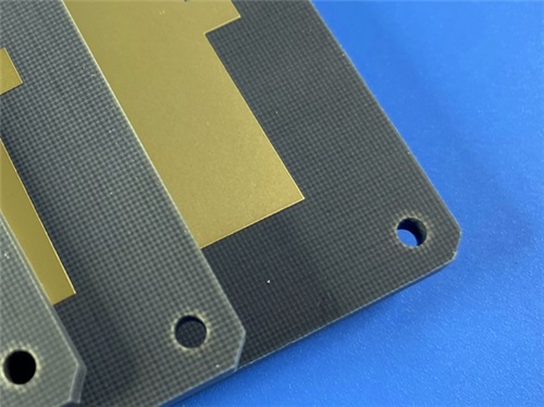
 custom TP PCB


Diverse Application Spectrum


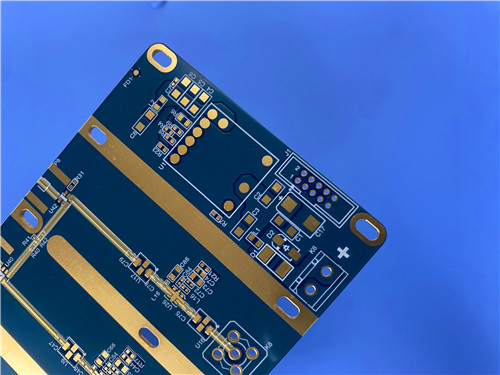
The robust combination of electrical and mechanical properties makes TP High Frequency PCBs indispensable in several high-stakes industries. A typical example is a 1.5mm thick TP PCB with an OSP (Organic Solderability Preservative) surface finish, commonly used in sophisticated communication systems. Beyond this, these PCBs are critically deployed in applications such as the Beidou satellite navigation system, missile-borne guidance systems, advanced radar fuzes, and miniaturized high-gain antennas. In each case, the material's stable electrical performance, thermal resilience, and reliability under harsh conditions ensure optimal system functionality.


Conclusion


For engineers pushing the boundaries of high-frequency and high-speed design, custom TP PCB offers a powerful combination of customizability, performance, and reliability. By enabling precise control over dielectric properties and providing robust performance in challenging environments, it serves as a foundational component for the next generation of aerospace, defense, and telecommunications technology. When your design demands uncompromising signal integrity, TP material provides a proven and capable solution.

How Does RO3203 Laminate Deliver Superior Electrical and Mechanical Performance Cost-Effectively?


Introduction

In the rapidly advancing world of wireless communication and high-speed electronics, the choice of printed circuit board (PCB) substrate material is paramount. For engineers and designers working on cutting-edge RF, microwave, and millimeter-wave applications, achieving optimal electrical performance without compromising mechanical reliability or budget is a constant challenge. Enter RO3203 high-frequency circuit materials, a superior class of laminates engineered to meet these exacting demands. As a strategic extension of the renowned RO3000 PCB series, Rogers RO3203 stands out by offering an exceptional balance of electrical properties, enhanced mechanical stability, and cost-effectiveness. This blog post provides a comprehensive exploration of the RO3203 material, its key characteristics, our advanced PCB fabrication capabilities, and its diverse application fields, illustrating why it is a premier choice for high-frequency designs.


The Properties of RO3203 Material

Rogers 3203 PCB is constructed as a ceramic-filled polytetrafluoroethylene (PTFE) composite laminate, reinforced with a woven fiberglass substrate. This specific engineering delivers a consistent and stable platform for high-frequency circuits.


The Properties of RO3203 Material


1) Superior Electrical Performance: The cornerstone of RO3203's appeal is its outstanding electrical properties. It boasts a stable dielectric constant (Dk) of 3.02, which remains consistent across a broad frequency spectrum. Coupled with an exceptionally low dissipation factor (Df) of 0.0016, this material ensures minimal signal loss and excellent signal integrity. These properties collectively enable reliable operation in an extended useful frequency range that surpasses 40 GHz, making it suitable for sophisticated millimeter-wave applications.


2) Enhanced Thermal and Mechanical Characteristics: Beyond electrical performance, RO3203 provides robust thermal and mechanical stability. Its thermal conductivity of 0.48 W/m/K contributes to effective heat dissipation from active components. The material demonstrates remarkable dimensional stability, with a value of 0.8 mm/m in both the X and Y axes, which is critical for maintaining registration in multilayer boards. Furthermore, its low moisture absorption rate of less than 0.1% ensures performance reliability even in humid environments. The material's coefficients of thermal expansion (CTE) are carefully controlled—13 ppm/°C in the X and Y directions and 58 ppm/°C in the Z-direction—which helps in minimizing stress during thermal cycling, such as in soldering processes.


3) Reliability and Durability: RO3203 is designed for long-term reliability. It features high volume and surface resistivity, both at 10^7 MΩ, ensuring excellent insulation properties. The copper peel strength after soldering is a robust 10.2 lbs/in, indicating strong adhesion between the copper foil and the substrate. With a Thermal Decomposition Temperature (Td) of 500°C and a UL 94 V-0 flammability rating, the material meets stringent safety and durability standards. Its full compatibility with lead-free assembly processes makes it a future-proof choice for modern electronics manufacturing.


Advanced PCB Manufacturing Capabilities for RO3203


As a leading PCB supplier, we possess the specialized expertise and equipment to fully leverage the advantages of RO3203 substrate. Our manufacturing capabilities are tailored to meet the precise requirements of high-frequency applications.


PCB Manufacturing Capabilities for RO3203


1) Versatile Board Constructions: We offer comprehensive solutions including single-layer, double-layer, complex multi-layer, and hybrid stack-up configurations. Hybrid designs allow for the integration of RO3203 with other materials, such as FR-4, optimizing performance and cost for specific sections of a circuit.


2) Flexible Specifications: To accommodate diverse design needs, we provide a wide range of options. This includes various standard and custom thicknesses (e.g., 10mil, 20mil, 30mil, 60mil) and copper weights (e.g., 1oz, 2oz). We can handle large-format boards up to 400mm x 500mm.


3) Comprehensive Finishing Options: We offer a full spectrum of surface finishes to protect the circuitry and ensure solderability. Choices include Bare Copper, HASL (Hot Air Solder Leveling), Immersion Tin (ImSn), Immersion Silver (ImAg), ENIG (Electroless Nickel Immersion Gold), OSP (Organic Solderability Preservative), Pure Gold, and ENEPIG (Electroless Nickel Electroless Palladium Immersion Gold). Additionally, a variety of solder mask colors like green, black, blue, yellow, and red are available for identification and protection.


Key Application Areas for RO3203 High Frequency PCBs


The unique property set of RO3203 PCB makes it an ideal substrate for a wide array of high-performance applications across multiple industries. Its primary use is in areas where signal speed and integrity are non-negotiable.


RO3203 PCB


1) Automotive Radar Systems: It is extensively used in advanced driver-assistance systems (ADAS), particularly in automotive collision avoidance and adaptive cruise control radar operating at 24 GHz and 77 GHz.


2) Telecommunications Infrastructure: RO3203 is perfect for GPS antennas, microstrip patch antennas, and base station antennas that require low loss and stable performance.


3) Satellite Communication: Its reliability makes it suitable for direct broadcast satellite (DBS) systems and other satellite communication equipment.


4) IoT and Smart Metering: Applications like remote meter readers and other RF-enabled IoT devices benefit from the material's consistent performance.


Conclusion


RO3203 high frequency PCB represents a technologically advanced and economically viable solution for designers pushing the boundaries of high-frequency electronics. Its blend of stable electrical properties, mechanical robustness, and thermal reliability, combined with our extensive manufacturing expertise, ensures that your next high-frequency project will be built on a foundation of quality and performance. For your upcoming designs requiring operation beyond 40 GHz, consider custom RO3203 PCB materialas your substrate of choice.


Contact us today to discuss your specific RO3203 Rogers PCB requirements and receive a competitive quote.

Seeking a High-Frequency PCB with Exceptional Dimensional Stability and Low Loss? Explore F4BTMS.


In the relentless pursuit of higher speeds and greater bandwidth within the electronics industry, the choice of printed circuit board (PCB) material becomes paramount. For applications operating at radio frequency (RF) and microwave ranges, standard FR-4 materials fall short, leading to significant signal degradation and loss. Enter the F4BTMS High Frequency PCB –a technologically advanced circuit board substrate engineered to meet the rigorous demands of next-generation high-frequency applications. This article delves into the superior properties, manufacturing capabilities, and diverse applications of Wangling F4BTMS, positioning it as an indispensable solution for engineers designing cutting-edge systems.


Evolution in Material Science: The Foundation of F4BTMS


The F4BTMS series laminates represents a significant evolution from its predecessor, the F4BTM PCB series. This next-generation material achieves a remarkable leap in performance through a sophisticated material composition. The key enhancement lies in the integration of a substantial volume of special nano-ceramics within a Polytetrafluoroethylene (PTFE) resin matrix, reinforced with an ultra-thin and ultra-fine fiberglass cloth. This strategic formulation is instrumental in minimizing the interstitial voids that typically contribute to electromagnetic wave interference. The result is a dramatic reduction in dielectric loss (Df) and a significant enhancement in the material's dimensional stability across a wide temperature range.


Furthermore, F4BTMS PCB exhibits a highly reduced anisotropy in its thermal expansion characteristics across the X, Y, and Z axes. This balanced CTE (Coefficient of Thermal Expansion) is critical for maintaining the integrity of plated through-holes (PTHs) during thermal cycling, thereby ensuring long-term reliability. These combined improvements unlock the potential for higher frequency operation, increased electrical strength, and improved thermal conductivity compared to standard high-frequency materials.


Unparalleled Material Properties for Peak Performance


The F4BTMS material boasts a set of electrical and thermal properties that make it stand out in the high-frequency PCB market:


F4BTMS features


1) Tunable and Stable Dielectric Constant (Dk): Offering exceptional flexibility, F4BTMS provides a wide range of dielectric constants from 2.2 to 10.2. More importantly, this Dk value remains exceptionally stable across the board, ensuring consistent signal propagation velocity and impedance control.


2) Extremely Low Dielectric Loss (Df): With a dissipation factor ranging from an ultra-low 0.0009 to 0.0024, F4BTMS ensures minimal energy conversion into heat. This low loss tangent is crucial for enhancing overall system efficiency, preserving signal strength, and enabling clearer signal transmission in sensitive applications.


3) Excellent Thermal Stability (TCDk): The Temperature Coefficient of the Dielectric Constant (TCDk) is a critical metric. For F4BTMS, with Dk values from 2.55 to 10.2, the TCDk remains within a tight±100 ppm/°C. This stability guarantees that electrical performance remains predictable and reliable even under fluctuating operational temperatures.


4) Superior Dimensional Stability (CTE): The CTE values are meticulously controlled—between 10-50 ppm/°C in the X and Y directions and a commendably low 20-80 ppm/°C in the Z direction. This low thermal expansion is fundamental to preventing delamination and ensuring reliable via connections.


5) Aerospace-Grade Reliability: F4BTMS demonstrates remarkable resistance to radiation, maintaining stable properties even after exposure. Its low outgassing performance meets the stringent vacuum outgassing requirements (as per ECSS-Q-ST-70-02C) essential for aerospace and satellite applications.


Comprehensive PCB Manufacturing Capabilities


F4BTMS PCB Manufacturing Capabilities


To fully leverage the advantages of the F4BTMS substrate, our manufacturing expertise is tailored to deliver precision and quality. We support a comprehensive range of PCB structures to suit diverse design requirements, including Single-Sided, Double-Sided, Multilayer, and Hybrid constructions. Our capabilities extend to various copper weights (e.g., 1oz/35µm, 2oz/70µm) and a diverse selection of dielectric thicknesses from a thin 0.09mm (3.5mil) to a robust 6.35mm (250mil). We can accommodate PCB sizes up to 400mm x 500mm and offer multiple solder mask colors (Green, Black, Blue, etc.) and surface finishes (ENIG, Immersion Silver, OSP, ENEPIG, and more) to meet both functional and aesthetic needs.


F4BTMS615 High Frequency PCBs


Broad-Ranging Applications


The exceptional properties of F4BTMS High Frequency PCBs make them the ideal choice for a multitude of advanced sectors. They are extensively used in:


Aerospace and Aviation Equipment (e.g., flight control systems, communication satellites)

Microwave and RF Applications (including 5G infrastructure and point-to-point radio)

Advanced Radar Systems

Signal Distribution and Feed Networks

Phase-Sensitive Antennas and Phased Array Antennas


In conclusion, the custom F4BTMS PCB is not merely an incremental upgrade but a transformative solution for high-frequency design challenges. Its superior electrical characteristics, exceptional thermal stability, and proven reliability make it the superior substrate for pushing the boundaries of performance in today's most demanding electronic systems.

Seeking a High-Performance, Reliable HF PCB Material? What Can F4BTM Offer Your Design?


In the rapidly advancing world of wireless technology, the demand for high-frequency printed circuit boards (PCBs) that offer exceptional electrical performance, unwavering reliability, and cost-effectiveness is greater than ever. Wangling F4BTM High Frequency PCB emerges as a premier solution engineered to meet these rigorous challenges head-on. This article delves into the unique composition, outstanding features, and extensive capabilities of F4BTM, illustrating why it is the material of choice for cutting-edge applications.


Advanced Material Composition: The Foundation of Excellence


The superior performance of Wangling F4BTM series laminates originates from its sophisticated material science. The base structure is composed of a robust fiberglass cloth reinforced with a proprietary blend of nano-ceramic fillers and Polytetrafluoroethylene (PTFE) resin. This combination is subjected to strictly controlled pressing processes to ensure consistency and quality. Building upon the proven F4BM dielectric layer foundation, the strategic incorporation of high-dielectric, low-loss nano-ceramic particles yields a composite material with significantly enhanced properties. The result is a laminate that exhibits a higher and more stable dielectric constant (Dk), superior heat resistance, a reduced coefficient of thermal expansion (CTE), elevated insulation resistance, and improved thermal conductivity, all while meticulously preserving the low-loss characteristics critical for high-frequency signal integrity.


Furthermore, the F4BTM PCB series offers versatility through its copper foil options. The standard F4BTM variant is paired with Electrodeposited (ED) copper foil, providing a reliable and cost-effective solution. For applications where performance is paramount, the F4BTME variant utilizes Reverse-Treated Foil (RTF). This choice delivers exceptional Passive Intermodulation (PIM) performance, enables more precise control over fine lines during etching, and contributes to lower overall conductor loss, making it ideal for sensitive RF systems.


Comprehensive Feature Set for Superior Design Flexibility


 F4BTM PCB's features


F4BTM PCB is distinguished by a wide array of features that provide engineers with remarkable design flexibility. Its stable Dielectric Constant (Dk) can be tailored within a range of 2.98 to 3.5, allowing for precise impedance matching and optimized circuit design for specific frequency bands. The nano-ceramic enhancement is pivotal, boosting the material's overall performance to suit the most demanding high-frequency and high-speed digital applications.


This high-performance material is available in a diverse selection of standard thicknesses and panel sizes, accommodating a broad spectrum of project requirements without necessitating custom orders, which translates into significant cost savings. Its formulation is designed for excellent manufacturability, supporting large-scale production runs with high yield, thereby establishing F4BTM as a highly cost-effective choice without compromising on quality. Additionally, F4BTM laminates possess radiation-resistant and low out-gassing properties, guaranteeing long-term reliability and functionality even in the harsh environments of aerospace and satellite applications.


Extensive PCB Manufacturing Capabilities


F4BTM PCB Manufacturing Capabilities


To fully leverage the advantages of F4BTM material, Wangling supports it with a comprehensive suite of advanced PCB manufacturing capabilities. We possess the expertise to produce a wide variety of board configurations, including single-sided, double-sided, complex multilayer, and hybrid PCBs that combine different materials.


We offer flexibility in copper weight, with standard options of 1oz (35µm) and 2oz (70µm), to meet varying current-carrying and conductivity requirements. For dielectric and overall board thickness, we provide an extensive selection ranging from a thin 0.25mm up to a substantial 12.0mm, catering to diverse mechanical and electrical design specifications. Our manufacturing lines can accommodate PCBs with maximum dimensions of 400mm x 500mm.


To support both functional and aesthetic needs, we offer solder mask in various colors, including green, black, blue, yellow, and red. For surface finish, we support all common and advanced types such as bare copper, HASL (Hot Air Solder Leveling), ENIG (Electroless Nickel Immersion Gold), immersion silver, immersion tin, OSP (Organic Solderability Preservative), pure gold, and ENEPIG (Electroless Nickel Electroless Palladium Immersion Gold).


F4BTM300 PCB


Diverse Application Spectrum


A prime example of F4BTM PCB in use is a circuit board designed with a DK of 3.0, constructed on a 1.524mm thick substrate and finished with HASL. The applicability of DK 3.0 F4BTM PCB is vast, covering critical sectors such as:


Antenna systems (including base station antennas)

Mobile Internet infrastructure

Sensor Networks and IoT devices

Radar and Millimeter Wave Radar systems

Aerospace and avionics

Satellite Navigation (GPS, GLONASS, Galileo, etc.)

Power Amplifiers for communication equipment


In conclusion, F4BTM High Frequency PCB stands as a testament to material innovation, offering an optimal balance of high performance, design versatility, manufacturing efficiency, and reliability. For your next project requiring superior signal integrity and robust operation in demanding conditions, custom F4BTM PCB provides a proven and cost-effective solution.